IPC-7095C-2013.pdf - 第92页
requirements are the same for both copper balls or high temperature 90Pb/10Sn balls since neither ball collapses during reflow and all the solder fillet requirement have to be met by the paste. There are ceramic BGAs that …
When making decisions about stencil thickness and volume
of paste to be deposited, it is safer to deposit more paste
than less paste with the goal of achieving six times more
bridges than opens (this is the ratio and not more defects).
The reasons are that bridges can rarely escape inspection
and they are sure to be caught by tests (ICT or functional).
Opens and intermittent opens, on the other hand, can easily
escape tests since they may make contact due to pressure
applied during testing but will result in field failures. So
this simple guideline to target more bridges than opens
while designing stencil and land patterns is the most cost
effective method to prevent field failures.
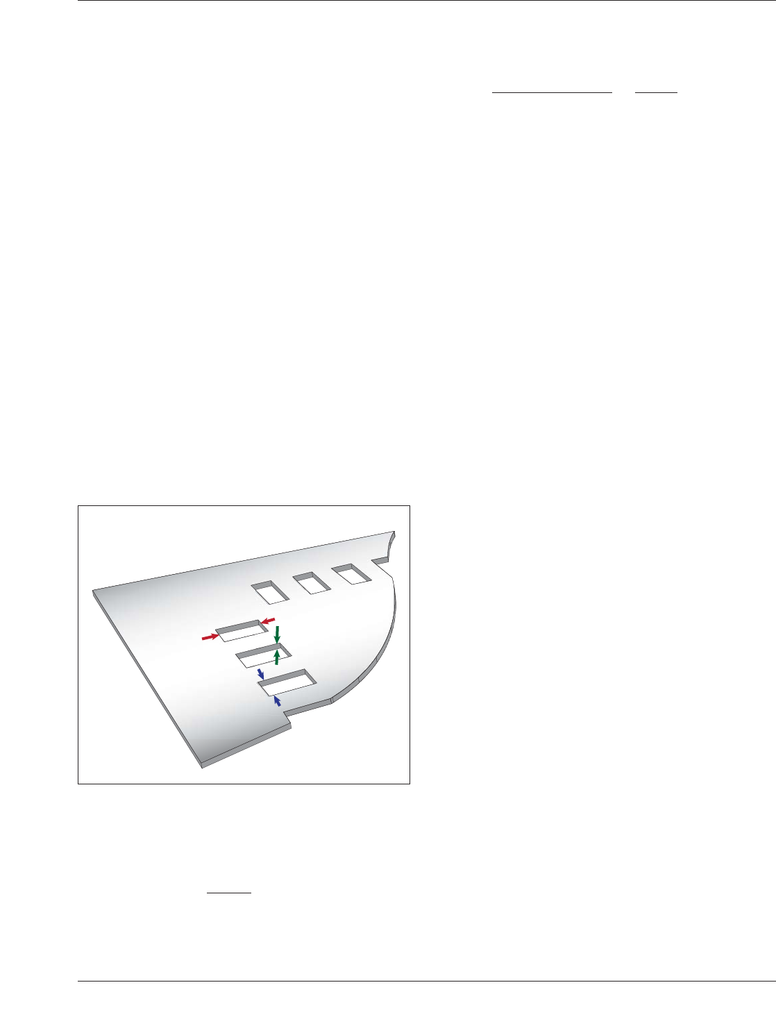
It is also very important to design a stencil aperture that
will provide good paste release. In order to ensure good
paste release, an aspect ratio of 1.5 is recommended.
Aspect ratio is the ratio between stencil aperture width and
stencil thickness. Another commonly used ratio is called
area ratio. An area ratio of greater than 0.66 is recom-
mended. The formula to calculate area aspect ratio is the
area of the stencil aperture divided by the area of the sten-
cil walls (see Figure 7-1). The idea behind designing sten-
cil with these strongly recommended aspect and area ratios
is to allow more paste release and minimize any paste
along the stencil walls which may partially clog apertures
and reduce paste volume on subsequent boards to be
printed next, resulting in insufficient solder joints or even
opens.
Area land contact/area stencil wall equals aperture/area of
aperture walls) = L*W/2*(L+W)*T >0.66
LxW
2(L+W)
xT
Note: Aspect ratio is more common than area ratio in
aperture design since aspect ratio is one dimensional sim-
plification of the area ratio when land length is much
greater than width i.e., a square aperture with a dimension
of 0.35 mm with a stencil thickness of 0.125 mm gives the
resulting aspect ratio:
0.35x0.35
2(0.35+0.35)x0.125
=
0.1225
0.175
= 0.70
Using an overprint or an aperture larger than the land may
be necessary to achieve this ratio, especially for finer pitch
BGAs, Stencil apertures are generally one to one or slightly
smaller than the land in order to achieve gasketing. When
and if the stencil apertures need to be larger than the lands,
to achieve the desired area ratio for better paste release,
cleaning of the stencil after each print may be necessary.
Larger apertures will cause paste to leak under the stencil
resulting in paste smudging on boards to be printed next. It
should also be noted that stencil apertures are significantly
larger than the lands when designing stencils for CBGAs,
CCGAs, and paste-in-hole processes.
A square or rectangular aperture with rounded corners will
also provide better paste release and volume deposition.
7.1.1.3 Importance of Paste Volume For plastic BGAs
much of their solder volume is supplied by the solder ball
on the part itself and the paste volume is not that critical.
For plastic BGAs (in both SnPb and lead-free configura-
tions) above 0.80 mm pitch, stencil thickness will be dic-
tated by the other component types used on the printed
board assembly. Solder volume and stencil thickness
become more critical for ceramic BGAs with noncollaps-
ible copper balls or high temp 90%Pb/10%Sn balls with
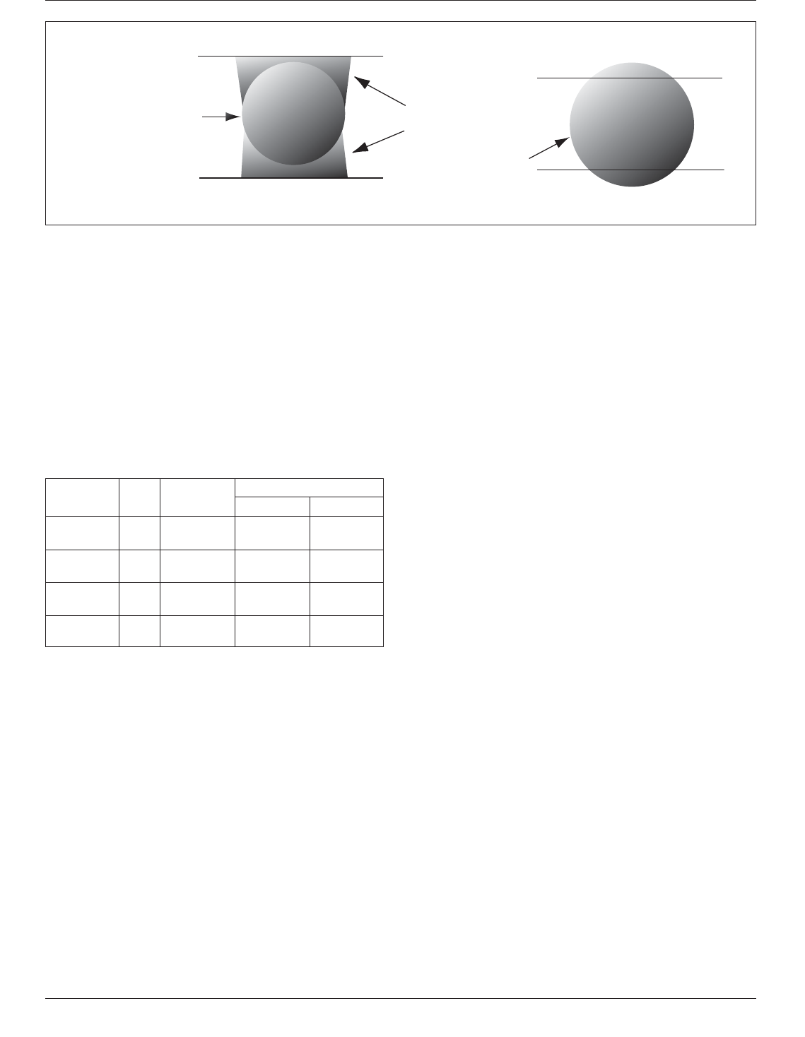
melting point of 302°C The solder balls used on ceramic
BGAs do not collapse during the normal reflow process
(see Figure 7-2).
For CBGA with noncollapsible balls (copper balls or 90Pb/
10Sn) where thicker solder volume is required, a stepped
stencil may be used. The step is typically 0.04 mm to
0.08 mm, and it can put two different paste thicknesses on
the board surface. A metal squeegee can be used success-
fully when the step is 0.04 mm. If a stepped stencil is used,
the step line should be at least 3.75 mm away from any
print aperture. Because the high lead content ball does not
collapse, having sufficient solder paste is critical. So in
addition to using stepped stencil, the stencil aperture may
also have to be much bigger than the land to achieve the
required paste volume for noncollapsible balls. The fillet
between the land and ball depend upon the solder paste
volume. Ceramic BGAs and CGAs require a minimum vol-
ume of solder pastes to make a reliable solder joint. There
are various suppliers of this type of technology who can
provide the specific solder paste volume for their package.
Table 7-2 contains an example of the solder paste volume
requirements for some of the ceramic packages using either
tin/lead or lead free (SAC) solder paste (see Table 7.2).
The paste volume requirements should be the same for
both tin/lead and lead free paste. Also the paste volume
IPC-7095c-7-1
Figure 7-1 Aspect and Area Ratios for Complete Paste
Release
Solder Stencil Feature Dimensions
Aperture length (L)
Stencil thickness (T)
Aperture width (W)
January 2013 IPC-7095C
77
Copyright IPC-Association Connecting Electronics Industries
Provided by IHS under license with IPC
Not for Resale
No reproduction or networking permitted without license from IHS
--`,,```,,,,````-`-`,,`,,`,`,,`---
requirements are the same for both copper balls or high
temperature 90Pb/10Sn balls since neither ball collapses
during reflow and all the solder fillet requirement have to
be met by the paste.
There are ceramic BGAs that do not use noncollapsible
balls and use lead free (SAC) solder balls that do collapse
during reflow and contribute towards the formation solder
fillet just as tin/lead balls do in plastic BGAs. The numbers
shown in Table 7-2 do not apply to either plastic or ceramic
BGAs that use collapsible balls.
In order to achieve the correct solder volume of solder
paste for a ceramic package with noncollapsible balls (cop-
per or Pb90/Sn10), it is necessary to overprint the land with
a larger aperture or use a thicker stencil. For other compo-
nents on a circuit board with CBGAs, the aperture size may
need to be adjusted to compensate for the thicker stencil or
it may be necessary to step the stencil.
7.1.2 Component Placement Impact Getting into BGA
technology also requires some new assembly capability.
Depending upon the type of pick and place system, a
change in package carrier mechanism may also be required
to transfer packages from matrix tray to the pick position.
Fiducials may help vision systems to recognize the exact
location of the land pattern for the BGA, similar to what is
used for fine-pitch peripheral leaded parts. Large BGA
parts on tape-and-reel will require 44 mm and 56 mm feed-
ers depending on the body size. However, most common
feeders for BGAs are JEDEC trays.
7.1.3 Vision Systems for Placement Placement accu-
racy is a very critical part of the BGA process. It is
strongly recommended to not move a BGA after machine
placement to correct placement problems as this may cause
solder bridging in adjacent solder joints, since the connec-
tions cannot be seen visually. The placement machine’s
accuracy is largely dependent on the vision system and the
ability of the nozzle to hold the component. Matching the
vision system to the application is also important. The
vision system determines the X, Y and theta offset of each
component prior to placement. In addition to determining
the component offset, the vision system can also inspect the
component for dimensional integrity and missing solder
balls. CCD (charge-coupled device) camera-based systems
employ two lighting methods, referred to as binary and
gray scale. Both methods can be sensitive to contrast and
lighting changes.
Gray scale systems use front lighting, which illuminates
the component from below. Surface features are reflected
into the CCD camera for processing. Binary systems use
back lighting, which illuminates the component from
above. The outline of the component is projected into the
CCD camera for processing. Binary imaging, which is the
older of the two methods, locates a feature using the con-
trast between black and white images. Gray scale systems
can usually interpret 256 levels of contrast. Both systems
use an algorithm to determine the center of the component.
Binary imaging requires less computing capability than
gray scale imaging.
Gray scale imaging places BGA components based on ball
location while binary imaging places BGA components
based on the component outline. In some cases the toler-
ance between the BGA outline and the balls is significant.
Gray scale imaging is more desirable for placing BGA
components because it eliminates placement error due to
variations in the component outline.
Placement machine nozzle designs vary from supplier to
supplier. It is important that the correct nozzle is chosen
which will have sufficient surface area to hold the part
without any shifting during the placement process. The
IPC-7095c-7-2
Figure 7-2 High Lead and Eutectic Solder Ball and Joint Comparison
PBGA Substrate
PWB
62Sn/36Pb/2Ag
b)
a)
CBGA Substrate
PWB
Eutectic Sn/Pb
90/10 Pb/Sn Ball
Table 7-2 Example of Solder Paste Volume
Requirements for Ceramic Array Packages
Component
Pitch
(mm)
Solder
Paste Alloy
Volume in µm
3
Low (min) High (max)
CBGA/
CuBGA
1.27
Tin/Lead or
Lead-free
78,660,000 163,870,000
CBGA/
CuBGA
1.00
Tin/Lead or
Lead-free
40,968,000 75,380,000
CCGA/
CuCGA
1.27
Tin/Lead or
Lead-free
60,632,000 124,542,000
CCGA/
CuCCGA
1.00
Tin/Lead or
Lead-free
32,321,000 81,935,000
IPC-7095C January 2013
78
Copyright IPC-Association Connecting Electronics Industries
Provided by IHS under license with IPC
Not for Resale
No reproduction or networking permitted without license from IHS
--`,,```,,,,````-`-`,,`,,`,`,,`---
nozzle must gasket against the part, not allowing vacuum
leakage. Tactile sensing, which helps control the Z axis
(vertical) stroke of the spindle, is desirable because it pre-
vents a component from being crushed between the
vacuum nozzle and the substrate.
7.1.4 Reflow Soldering and Profiling Reflow soldering
is a complex process with many variables. All mass reflow
systems incorporate convective, conductive and radiant
means of heat transfer, to what degree depends on the
design of the reflow system. All designs strive to achieve
the same fundamental results. Five different phases take
place during reflow. The five phases are: (1) evaporate sol-
vents from the solder paste, (2) activate the flux and allow
fluxing action to occur, (3) preheat the components and
printed circuit board, (4) melt the solder and allow proper
wetting to occur, and (5) cool the soldered assembly.
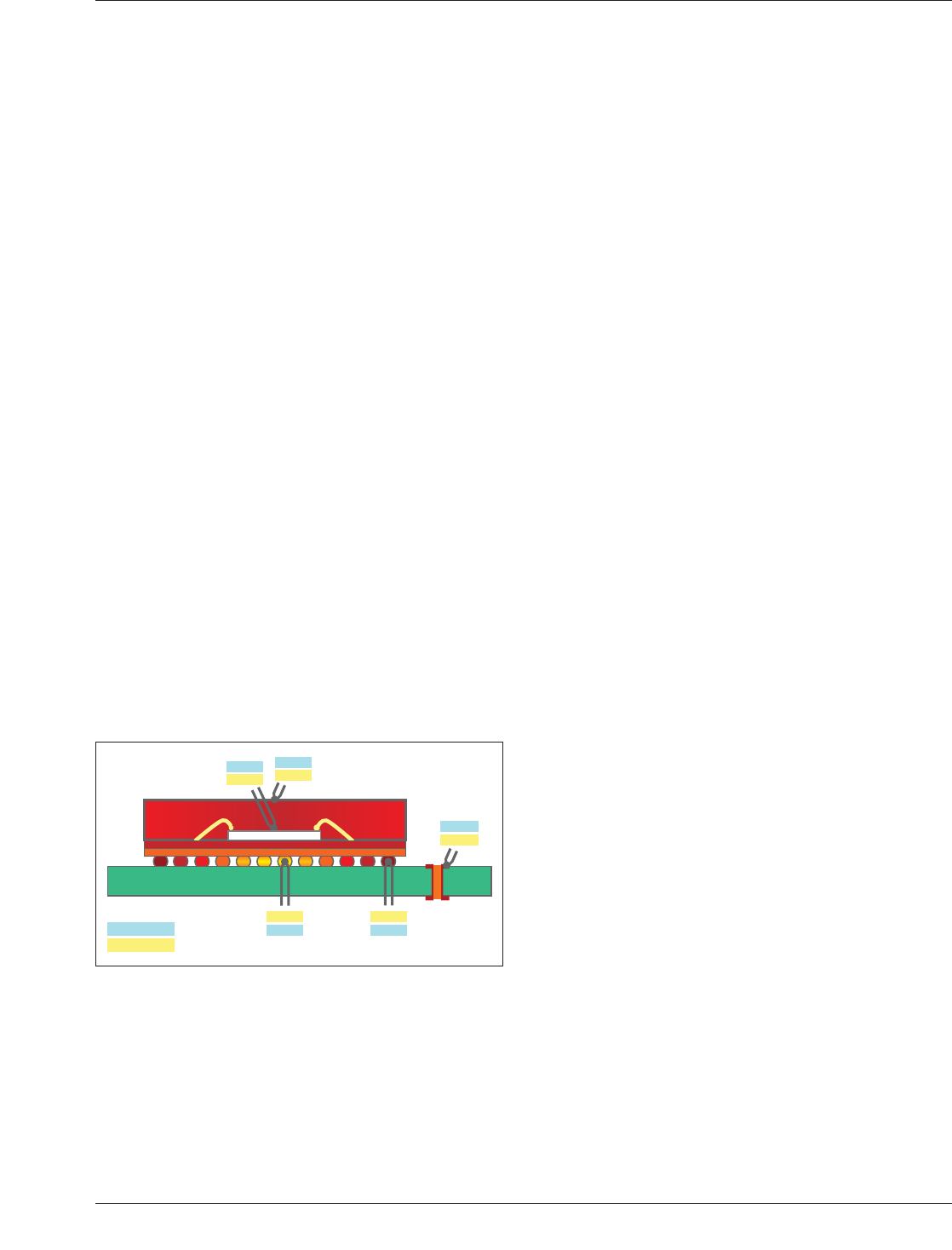
It needs to be understood that, regardless of the basic
reflow heat transfer concept used, the solder balls under-
neath a BGA component are primarily heated by conduc-
tive heating through the interconnect substrate. The reason
for this is illustrated in Figure 7-3. The optimal reflow pro-
file (temperature vs. time) including the peak temperature
varies with the specific package and the overall assembly.
However, as a guideline, when using SAC305 solder paste
for BGA packages containing SAC305 solder balls, the
minimum peak temperature for moderately complex
PCBAs may need to be not lower than approximately
240°C. When using tin/lead eutectic solder paste for BGA
packages containing SAC305 solder balls, the minimum
peak temperature in most cases can be as low as approxi-
mately 215°C. (See Table 7-3 for recommendations for
proper reflow temperatures.)
Over the years, reflow equipment has changed frequently.
Five design concepts have been used: vapor phase, lamp
infrared (IR), panel IR, and forced gas convection and
diode laser. Vapor phase reflow technology evolved first
and was popular for a few years. Eventually, IR became the
preferred approach. Today, forced gas convection (95% of
total heat source) with IR assist (5% of total heat source)
technology is the method of choice with some applications
requiring an inert oven atmosphere. Diode laser soldering
is the newcomer to the industry and used mostly in high
end high reliability applications such as space, military and
medical industries.
7.1.4.1 Forced Gas Convection Convection heat is
today’s method of choice. Heat is transferred to the printed
circuit assembly (PCA) by low velocity heated gas. Forced
gas convection is a noncontact heating method, with some
heating accomplished by radiation. The rate at which heat
is transferred to the object is directly proportional to the
difference in temperature between the heated gas and the
PCA.
Inline forced gas convection systems have three main sec-
tions: (1) preheat, (2) reflow and (3) cooling. Each section
contains a number of top and bottom zones. The number of
zones has a direct effect on the transport speed and the
user’s ability to fine tune the profile. Adding more zones
allows the user to run a faster belt speed and it permits
more flexibility in accurate profiling. Low volume reflow
systems have three or four zone sections (a zone section
includes top and bottom heaters). Medium volume reflow
systems have five or six zone sections, while the higher
volume systems use seven or more. Typically, a six zone
system will satisfy most reflow requirements, including
very large PCAs and reasonably high transport speeds (up
to 60 cm per minute). Profile changes are accomplished by
adjusting the transport speed and top and bottom tempera-
ture settings.
7.1.4.2 Reflow Atmosphere The atmosphere of the
reflow furnace will affect solder wetting. Reflowing in a
nitrogen environment will result in improved wetting of the
solder joint. This will sometimes allow compensation for
marginally wettable surfaces on the boards as well as oxi-
dized solder balls. In order to obtain the maximum benefit
of the solder paste in a nitrogen environment, it is recom-
mended to monitor the oxygen content and control it within
the limits you have established for your process.
With the migration of products into lead-free technology,
the solderability of the lead-free solder pastes is not as
good as that of tin lead. It is also possible to use up the
activators in the solder paste to clean the oxides off the
paste, land, and balls prior to reflow if paste selection is not
made correctly. This would result in a nonuniform shaped
solder joint and possibly nonwetting of the land. Some sol-
der paste formulations may also be affected by reflow
atmosphere in the formation of voids. When using lead-free
processes with OSP surface finishes, it may be desirable to
reflow the product using nitrogen, especially for hole fill
problems in mixed assemblies. Hole fill problems can be
encountered in lead-free process especially when using no
clean flux and 1
st
or 2
nd
generation OSPs. Use of water
soluble aggressive fluxes and 3
rd
generation OSP should
help minimize hole fill problems.
IPC-7095c-7-3
Figure 7-3 Example of Peak Reflow Temperatures at Vari-
ous Locations at or Near a BGA
220°C
240°C
245°C
for LF-solders
230°C
235°C
260°C
225°C
for Sn/Pb
205°C 217°C
230°C
January 2013 IPC-7095C
79
Copyright IPC-Association Connecting Electronics Industries
Provided by IHS under license with IPC
Not for Resale
No reproduction or networking permitted without license from IHS
--`,,```,,,,````-`-`,,`,,`,`,,`---