IPC-7095C-2013.pdf - 第127页
7.8.8 Defect Correlation/Process Improvement It is important to use inspection information to control the manufacturing process to maximize quality and yield. The manufacturing process leaves a signature (acceptable or u…
reflow. Non-coalesce of solder particles are seen, which
indicates that solder paste does not have good oxidation
resistance in the conditions it was reflowed.
7.8.5.4 How to Mitigate HoP Problem HoP is not an
easy defect to solve since there are many failure modes that
can cause this defect. In many cases, the HoP problem
consists of more than one failure mode at a time. The best
problem-solving approach would be to identify which are
the primary failure modes that need to be addressed to
eliminate HoP.
When a HoP problem exists, increasing solder paste vol-
ume will decrease the incidence of HoP. It may require
overprinting solder paste on some or all lands.
Some of the reflow parameters that have impact on HoP are
peak temperature and TAL. When dealing with HoP
defects, increasing TAL and peak temperature can decrease
the defect level by adding more time for the package to
contact the paste after full collapse and coalesce. One other
reflow parameter that could have an impact on HoP is soak
time. The impact depends on the type of paste used and its
behavior in high temperature. Follow the paste manufac-
ture recommendations and be sure not to stress and dry the
flux before reflow.
Using nitrogen in the reflow oven has been used to reduce
oxidation and increase SMT yield for HoP.
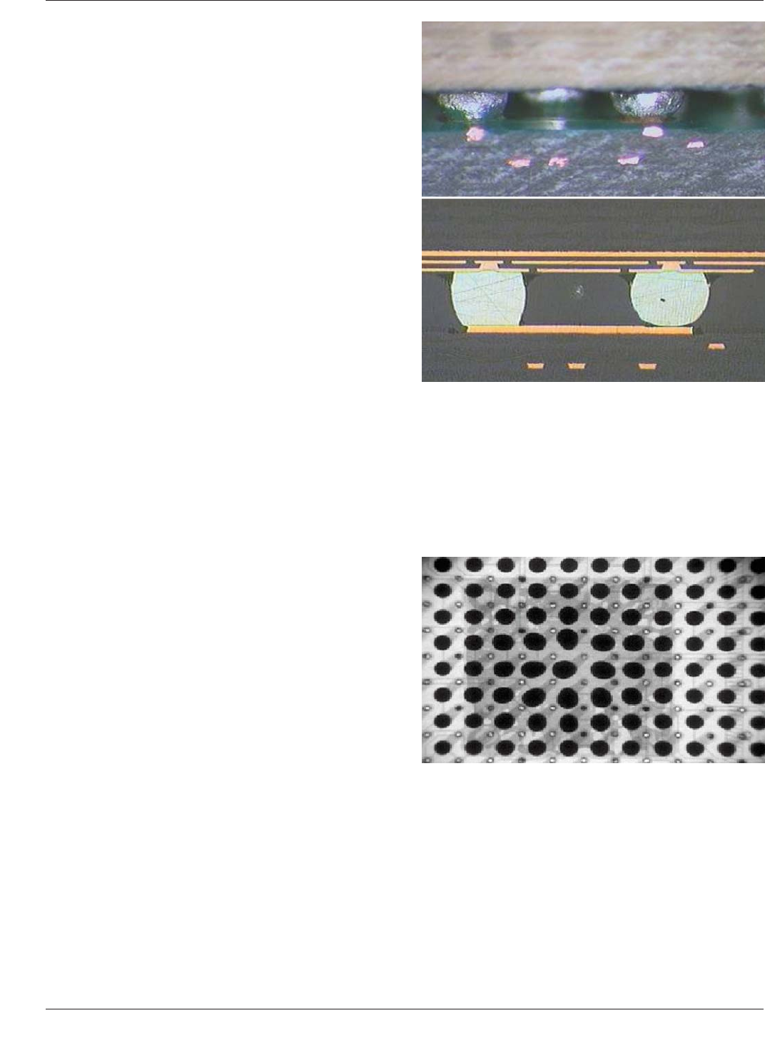
7.8.6 Hanging Ball/Non-Wet Open (NWO) A common
failure signature that is similar to head on pillow is head
with no pillow, which is known as nonwet open or hanging
ball. Failure happens in packages with high warpage. The
solder paste on the land adheres to the ball instead of
remaining on the land where it is supposed to be during
reflow. Because of package warpage, a gap is formed
between the package ball and the solder paste and the sol-
der sticks to the ball and coalesces with the ball. Oxide
builds up on the PCB land since it is exposed to high tem-
perature of reflow without the protection of flux resulting
in open joint known as hanging ball. Usually there is no
IMC formed on the land and it has the appearance of never
having any printed paste on it (see Figure 7-54).
Various factors affect hanging ball defects. They are type of
paste and flux, board land surface finish (OSP), land design
(SMD vs. MD) and copper on inner layers (thermal/ground
planes). To reduce occurrence of hanging balls, one should
change to a different solder paste chemistry, or add more
paste volume, or use nitrogen; all the solutions common to
HoP. Increasing the BGA land size also reduces hanging
ball incidence since a larger paste area provides more sur-
face tension and holds on to the paste instead of letting the
balls take the paste with them.
7.8.7 Component Defects Component defects such as
popcorning and warpage are generally caused by improper
handling of the BGA component prior to reflow. Both of
these problems produce a characteristic signature in the
X-ray image. Popcorning causes the BGA package to
expand below the die; resulting in an increase in size (and
possibly bridging) of the solder balls in the center of the
package as they are squished between the package and the
board (see Figure 7-55).
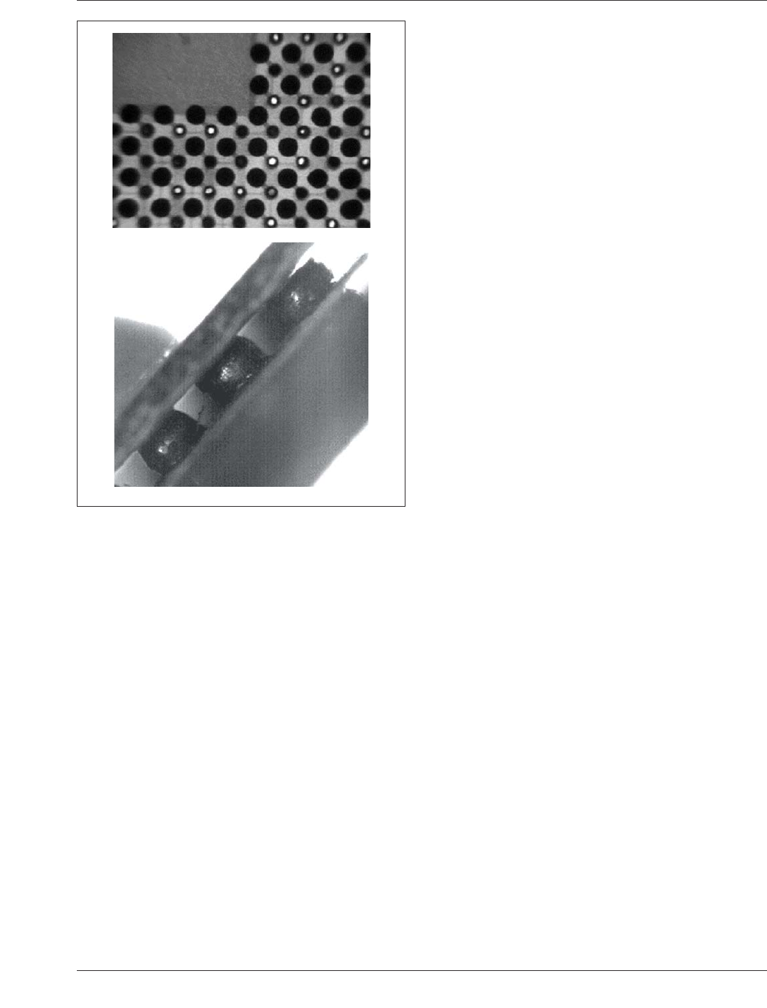
BGA warpage is more subtle than popcorning and can be
more difficult to detect in an X-ray image (see Figure
7-56). Warpage tends to be the largest at the corners of the
package. The X-ray image of a warped BGA tends to have
large elongated solder connections at the corner of the
package where warpage has occurred. The illustration in
Figure 7-56a shows the X-ray image and Figure 7-56b
shows a video microscope image of the package. Note that
in Figure 7-56b the ripple in the substrate, which is char-
acteristic of a stress relief which likely occurred during
reflow.
Figure 7-54 Hanging Ball Examples
Figure 7-55 X-Ray Image of Popcorning
IPC-7095C January 2013
112
Copyright IPC-Association Connecting Electronics Industries
Provided by IHS under license with IPC
Not for Resale
No reproduction or networking permitted without license from IHS
--`,,```,,,,````-`-`,,`,,`,`,,`---
7.8.8 Defect Correlation/Process Improvement It is
important to use inspection information to control the
manufacturing process to maximize quality and yield. The
manufacturing process leaves a signature (acceptable or
unacceptable) on each component; this signature can be
observed through inspection. The signature can be
observed using methods and tools discussed previously.
In many cases a visual inspection of a BGA is the first clue
to any problems. An operator can look at the edge of the
BGA on all four sides. The distance between the BGA and
the circuit board should appear uniform and the solder balls
should appear consistent in shape.
To directly observe the solder connections under a BGA,
X-ray or optical inspection (endoscope) is necessary. These
methods can be used to inspect for obvious defects such as
bridges and missing balls. They are also useful for charac-
terizing the BGA reflow process. During inspection the
BGA solder balls should be examined for uniformity of
size and shape. In the absence of wetting indicators, the
solder balls should appear round and of equal size through-
out the package. A PBGA with a 0.75 mm diameter ball
prior to reflow will swell to a nominal 0.90 mm diameter
after reflow; a 36% increase. A 10-15% variation in solder
ball area from the center to the edge of the package is nor-
mal, but a larger variation can indicate a problem with the
reflow process.
X-ray inspection of the BGA from an angle is also useful
to examine the shape of the BGA solder ball in the area at
which it makes contact with the land. By changing the
angle of X-ray inspection, the land is shifted so that it does
not obscure the rest of the solder ball. This allows the
operator to inspect the shape of the solder connection as it
forms onto the land to verify that the land is in contact with
the solder ball and the solder is completely wetted to the
land.
Quantitative measurement of the solder bond X-ray image
can be performed using image analysis software. Such soft-
ware is useful, but not required for the inspection of BGAs.
The advantage of the software is in its ability to identify
and display subtle variations in the size and shape of the
solder bond image which is not easily observed by an
operator. These subtle variations are a signature of the
process used to manufacture the part and can be used to
monitor the process and to correct for deficiencies. A num-
ber of signatures can be correlated with known process
deficiencies.
7.9 Repair Processes
7.9.1 Rework/Repair Philosophy
Plastic ball grid arrays
are a forgiving component package. With their self align-
ment characteristics, a ball grid array can be placed as
much as 50% ball off land and when reflowed, the package
will properly align itself. With a controlled process and
appropriate equipment, rework should be kept to a mini-
mum.
There are many rework systems on the market, most of
which use a prism for placement, which allows the view-
ing of the land pattern on the board with the ball image
superimposed over it. Most systems also allow board pre-
heat and stored reflow profiles for many different compo-
nent sites. This section will focus on conditions that should
be met in order to successfully rework a plastic BGA.
There are four main rework functions for BGAs: removing
the component, redressing the site, placing the component,
and reflowing the component. These will be discussed in
the following paragraphs.
7.9.2 Removal of BGA When removing a BGA a deci-
sion has to be made regarding whether the component will
be reballed and used again or simply discarded. Special
considerations need to be made if the BGA will be reballed
and reused, i.e., maximum number of reflow cycles as rec-
ommended by the component vendor. Typically 3 reflows
IPC-7095c-7-56a.b
Figure 7-56 X-Ray Image Showing Warpage in a BGA
The x-ray image (a) shows a distortion of the ball bonds in the lower
right corner; characterized by large elongated bonds. The same
location as viewed through a visual microscope (b) shows warpage
and the solder ball peaking away from the package.
(a)
(b)
January 2013 IPC-7095C
113
Copyright IPC-Association Connecting Electronics Industries
Provided by IHS under license with IPC
Not for Resale
No reproduction or networking permitted without license from IHS
--`,,```,,,,````-`-`,,`,,`,`,,`---
is the maximum recommendations, so reballing a removed
BGA and reinstalling it would exceed this number. There-
fore, a reballed BGA will always exceed this limit. Many
OEMs do not allow re-balled BGAs, or re-use of any com-
ponent. One should check with the customer before pro-
ceeding.
If the component is to be reused and it is overmolded plas-
tic, it will have to be baked. These packages are nonher-
metic and therefore absorb water if they have been out of
a moisture controlled atmosphere longer than the time
allowed in J-STD-020. The baking process drives off mois-
ture and prevents the ‘‘popcorning effect,’’ which is water
vaporizing within the component during reflow and caus-
ing catastrophic failure. Another consideration before
removal concerns the components adjacent to the BGA. If
hot air is used, and if the profile to be used exceeds 4°C per
second, the components surrounding the BGA may need to
be shielded due to thermal shock or secondary reflow.
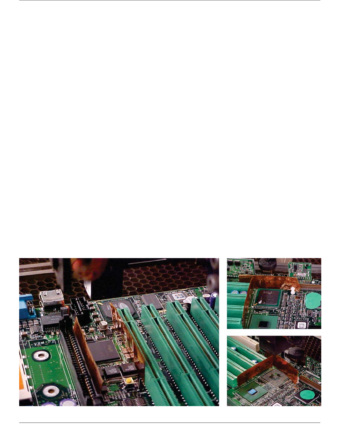
Polyimide tape or water soluble mask that is commonly
used in the wave solder processes can be used as shielding.
These deficiencies can be resolved with proper equipment
design. See Figure 7-57 for shielding with polyimide tape
to prevent damage to adjacent components when using hot
air for BGA repair.
With lead-free technology, it is recommended to minimize
the temperature delta between the bottom side of the board
and topside of the board during the profiling process for
BGA removal and reattach. The temperature of the bottom
side of the board heating should be increased to minimize
the topside nozzle heat when setting up the profile. This
will minimize exposure of potential delamination of the
bare board or heat transfer to adjacent components.
7.9.3 Replacement
7.9.3.1 Land Pattern Site Dressing
Once the BGA has
been removed from the board, solder will have to be
removed from the land pattern. Solder vacuums and solder
wick works well for removing solder off the lands. Caution
is recommended when using any of these tools because the
land can lift with excessive heat or pressure. Each land
must be completely flat and clean before placing the new
BGA. With the higher temperatures of lead-free alloys, it is
critical to minimize contact with the solder mask dams
between the lands and the vias (dog bone design). The
higher temperatures may increase the potential to damage
this solder mask. It can also be affected by the surface fin-
ish of the bare board. Two variables that can influence the
adhesion of the solder mask to the land are the length of
the solder mask dam (encroached vias are recommended)
and the surface finish of the bare printed boards.
7.9.3.2 Flux Application Although the solder mask
encroached on the via land is over bare copper, adhesion
can be affected when subjected to the surface finish chem-
istry.
Two different methods of flux application can be used:
paste/liquid flux or solder paste; however, using flux only
(in a liquid or paste form) is only applicable for eutectic
BGA reattachment. In addition, some applications require
the addition of solder paste in order to promote a robust
solder joint. If paste flux (also called tack flux) is to be
used ensure that the solder balls are Sn63/Pb37 (eutectic).
Many ceramic BGAs use Pb90/Sn10 solder balls which
reflow at 302°C. If the solder balls are not Sn63/Pb37, then
solder paste has to be used. If solder balls are SN63/Pb37,
Figure 7-57 BGA/Assembly Shielding Examples
IPC-7095C January 2013
114
Copyright IPC-Association Connecting Electronics Industries
Provided by IHS under license with IPC
Not for Resale
No reproduction or networking permitted without license from IHS
--`,,```,,,,````-`-`,,`,,`,`,,`---