IPC-7095C-2013.pdf - 第165页
Appendix A Process Control Characterization to Reduce the Occurrence of Voids In regard to voids and the percentage of voids within the ball, location of the voids is of greater concern. There is no evidence or empirical…

11 BIBLIOGRAPHY AND REFERENCES
ANSI/IPC-MF-150F, ‘‘Metal Foil for Printed Wiring Appli-
cations,’’ The Institute for Interconnecting and Packaging
Electronic Circuits, Lincolnwood, IL, October 1991.
Attarwala, A. I., and R. Stierman, ‘‘Failure Mode Analysis
of a 540 Pin Plastic Ball Grid Array,’’ Proc. Surface Mount
International Conf., San Jose, CA, August-September 1994,
pp. 252-257.
Bogatin, E., ‘‘BGAs for Workstation Application,’’ Proc.
Ball Grid Array Nat. Symp., Dallas, TX, March 1995.
Davignon, John, and Gray, Foster. ‘‘An evaluation of via
hole tenting with solder mask designed to pass Mil-P-
55110D thermal shock requirements.’’ Proceedings of
Technical Program SMI 91, San Jose, August 25-29, 1991,
pp. 905-921.
Denkler, J. D. ‘‘The speed of liquid.’’ Circuits Manufactur-
ing, May 1986, pp. 21-24.
D. Hillman, D. Adams, T. Pearson, B. Williams, B. Petrick,
R. Wilcoxon, Rockwell Collins; and D. Bernard, J. Travis,
E. Krastev, V. Bastin, Nordson Dage, ‘‘The Last Will and
Testament of the BGA Void,’’ SMTA International 2011.
Engelmaier, W., and B. Fuentes, ‘‘Alloy 42: A Material to
be Avoided for Surface Mount Solder Component Leads
and Lead Frames,’’ Proc. Surface Mount International
Conf., San Jose, CA, August-September 1994, pp. 644-
655; also in Proc. Int. Electronics Packaging Conf. (IEPS),
Atlanta, September 1994, pp. 503-516.
Engelmaier, W., ‘‘Reliability Figures of Merit for Surface
Mount Solder Attachments of Components: 2nd Generation
Generic Design Tools,’’ Proc. Surface Mount International
Conf., San Jose, CA, August 1991, pp. 1239-1243.
Engelmaier, W., ‘‘Solder Joint Reliability for BGAs and
Other Advanced Electronic Components,’’ Workshop
Notes, Engelmaier Associates, L.C., Ormond Beach, FL,
1999.
Greg Hillman, DfR Solutions, Long-term reliability of
Pb-free electronics (Kirkendall Voiding) hhtp://www.
electronicproducts.com/rohs/?filename+dfr. sep2005.html
Hines, L. L., ‘‘SOT-23 Surface Mount Attachment Reliabil-
ity Study,’’ Proc. 7th Annual Int. Electronics Packaging
Conf. (IEPS), Boston, MA, November 1987, pp. 613-629.
Hwang, J. & Kho, V., ‘‘Lead-free Implementation: Drop-In
Manufacturing,’’ APEX Conference Proceedings, 2004, pp.
S40-2-1 to S-40-2-13.
Hwang, J., ‘‘Environment-Friendly Electronics: Lead-free
Technology,’’ ISBN 0 901150 401, Electrochemical Publi-
cations LTD, 2001, p. 242 and pp. 64-105.
IPC-TR-462, ‘‘Solderability Evaluation of Printed Boards
with Protective Coatings over Long Term Storage,’’ Octo-
ber 1987, IPC Publications.
John Lau, ‘‘Ball Grid Array Technology’’ 1995. p.122.
Shows a graph of relative PCB cost per layer count.
Katchmar, R., ‘‘Position Dependence of CTE in Plastic
Ball Grid Arrays,’’ Proc. Int. Electronics Packaging Conf.
(IEPS), Atlanta, September 1994, pp. 271-283.
Lebonheur, C. Matayaba, S. Houle, and Y. Xu, Thermal
Interface Material Development, Intel Assembly & Test
Technology Journal, Vol 3, 2000.
Mawer, A. J., S. C. Bolton, and E. Mammo, ‘‘Plastic BGA
Solder Joint Reliability Considerations,’’ Proc. Surface
Mount International Conf., San Jose, CA, August-
September 1994, pp. 239-251.
NCMS, Lead-free Solder Project Final Report, August
1997, www.ncms.org.
Orsten, G. S. F., ‘‘The Problems Associated with Adhesive
Bonding of Components on Surface Mount Assemblies,’’
Proc. 19th Ann. Electronics Manufacturing Seminar, China
Lake, CA, February 1995, pp. 153-163.
Orsten, G. S. F., W. New, Y. Wang, and M. L. Peloquin
‘‘SMT Considerations in Spaceflight and Critical Military
Applications,’’ Proc. 18th Ann. Electronics Manufacturing
Seminar, China Lake, CA, February 1994, pp. 75-89.
Phelan, G., and S. Wang, ‘‘Solder Ball Connection
Reliability Model and Critical Parameter Optimization,’’
Proc. 43rd Electronic Components and Technology Conf.,
Orlando, FL, June 2-4, 1993, pp. 858-862.
Ref: Robert Crowley, Chip Scale Review, May 1998,
p. 37).
Rukavina, J., ‘‘Ball Grid Array Attachment Methodolo-
gies,’’ Proc. Ball Grid Array Nat. Symp., Dallas, TX,
March 1995.
Theo I. Eijm, Albert Holliday, Frank E. Bader and Steven
Gahr. AT&T Bell Laboratories, Princeton, NJ. ‘‘Designed
Experiment to Determine Attachment Reliability Drivers
for PBGA Packages.’’
‘‘Thermal and Power Cycling Limits of Plastic Ball Grid
Array (PBGA) Assemblies,’’ Robert Darveaux and Andrew
Mawer, Motorola.
IPC-7095C January 2013
150
Copyright IPC-Association Connecting Electronics Industries
Provided by IHS under license with IPC
Not for Resale
No reproduction or networking permitted without license from IHS
--`,,```,,,,````-`-`,,`,,`,`,,`---
Appendix A
Process Control Characterization to Reduce the Occurrence of Voids
In regard to voids and the percentage of voids within the
ball, location of the voids is of greater concern. There is no
evidence or empirical data that indicates that voids within
the ball will cause failure. Voids at the interface between
the ball-and-package substrate as well as voids at the inter-
face between the ball and the PCB will be more likely to
contribute to solder joint cracking. This is because cracks
(if they occur) will typically occur at the interface and the
void or voids can provide (in time) a path to accelerate the
cracking condition.
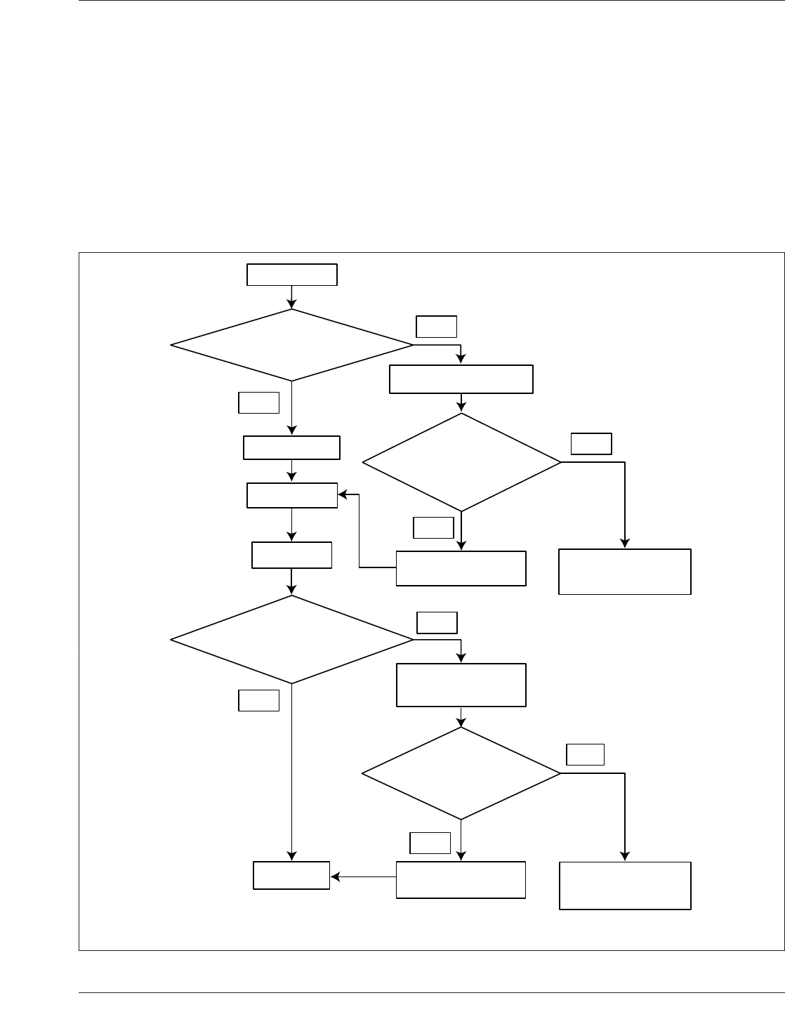
The determination of the impact that voids have on the
final product can best be expressed in terms of the flow
diagram shown in Figure A-1. See Tables A-1 to A-3 for
corrective action indicators.
IPC-7095c-a-1
Figure A-1 Typical Flow Diagram for Void Assessment
Inspect PCA
Any Balls with Voids Larger
than Maximum Void Size?
Ship PCA
More Voided Balls than
Allowable Percentage?
No Process
Action Required
Yes
No
Replace BGA and
Sample Inspect
Assembly Lot
No
Yes
Assemble PCA
No
Inspect BGAs
BGAs Pass Inspection Criteria
More Voided Balls than
Allowable Percentage?
No Process
Action Required
Take Appropriate
Corrective Action for
Product Class
Sample Inspect
Component Lot
No
Yes
Ship BGAs
Note: Sampling rates for void inspection to be determined by product requirements.
Yes
Take Appropriate
Corrective Action for
Product Class
January 2013 IPC-7095C
151
Copyright IPC-Association Connecting Electronics Industries
Provided by IHS under license with IPC
Not for Resale
No reproduction or networking permitted without license from IHS
--`,,```,,,,````-`-`,,`,,`,`,,`---

Table A-1 Corrective Action Indicator for Lands used with 1.5, 1.27 or 1.0 mm Pitch
Void
Type Void Description
Corrective Action Indicator
Action TakenClass 1 Class 2 Class 3
Determined by cross section/X-ray laminography
(sampling according to Section 7.6.3) at Component Incoming Evaluation
A Voids within the
solder ball (prior
to assembly)
Up to 90% balls may have voids
Maximum Void size in any ball is 20% of Area
(45% of the image diameter)
Investigate root
cause in process &
take corrective action
B Voids at package
interface (prior to
assembly)
Up to 80% balls may
have voids
Maximum Void size
in any ball is 15% of
area
(40% of the image
diameter)
Up to 70% balls may
have voids
Maximum Void size
in any ball is 10% of
area
(32% of the image
diameter)
Up to 50% balls may
have voids
Maximum Void size in
any ball is 5% of area
(22% of the image
diameter)
Investigate root
cause in process &
take corrective action
All balls with cumulative voids no matter what size are considered
Determined by cross section/X-ray laminography
(sampling according to Section 7.6.3) Evaluation after Assembly
C Voids within the ball
after PCA reflow
Up to 100% balls may have voids
Maximum Void size in any ball is 25% of Area
(50% of the image diameter)
Investigate root
cause in process &
incoming parts, take
corrective action
D Voids at the package
interface after PCA
reflow
Up to 100% balls
may have voids
Maximum Void size
in any ball is 25% of
area
(50% of the image
diameter)
Up to 80% balls may
have voids
Maximum Void size
in any ball is 20% of
area
(45% of the image
diameter)
Up to 60% balls may
have voids
Maximum Void size
in any ball is 15% of
area
(40% of the image
diameter)
Investigate root
cause in process &
incoming parts, take
corrective action
All balls with cumulative voids no matter what size are considered
E Voids at the mounting
surface interface after
PCA reflow
Up to 100% balls
may have voids
Maximum Void size
in any ball is 25% of
area
(50% of the image
diameter)
Up to 80% balls may
have voids
Maximum Void size
in any ball is 20% of
area
(45% of the image
diameter)
Up to 60% balls may
have voids
Maximum Void size
in any ball is 15% of
area
(40% of the image
diameter)
Investigate root
cause in process &
incoming parts, take
corrective action
Balls with cumulative voids smaller than 2% of the area (15% of the
image diameter) are not counted
Determined by transmission X-ray (sampling according to Section 7.6.3)
for Process Evaluation either at Component Incoming or after Assembly
A, B Voids at incoming Up to 80% balls may
have voids
Maximum Void size
in any ball is 15% of
area
(40% of the image
diameter)
Up to 70% balls may
have voids
Maximum Void size
in any ball is 10% of
area
(32% of the image
diameter)
Up to 50% balls may
have voids
Maximum Void size in
any ball is 5% of area
(22% of the image
diameter)
Investigate root
cause in process &
take corrective action.
All balls with cumulative voids no matter what size are considered
C, D, E Voids after PCA
reflow
Up to 70% balls may
have voids
Maximum Void size
in any ball is 25% of
area
(50% of the image
diameter)
Up to 60% balls may
have voids
Maximum Void size
in any ball is 25% of
area
(50% of the image
diameter)
Up to 50% balls may
have voids
Maximum Void size
in any ball is 20% of
area
(45% of the image
diameter)
Investigate root
cause in process &
incoming parts, take
corrective action
IPC-7095C January 2013
152
Copyright IPC-Association Connecting Electronics Industries
Provided by IHS under license with IPC
Not for Resale
No reproduction or networking permitted without license from IHS
--`,,```,,,,````-`-`,,`,,`,`,,`---