IPC-7095C-2013.pdf - 第71页
The following relationship can be used to determine the number of conductors per outlet for an interspersed array . C = [( r − 2 )( c − 2 )+( r − 1 )( c − 1 )]− d 2 ( r + c − 2 ) If C turns out to be a fraction, then rou…
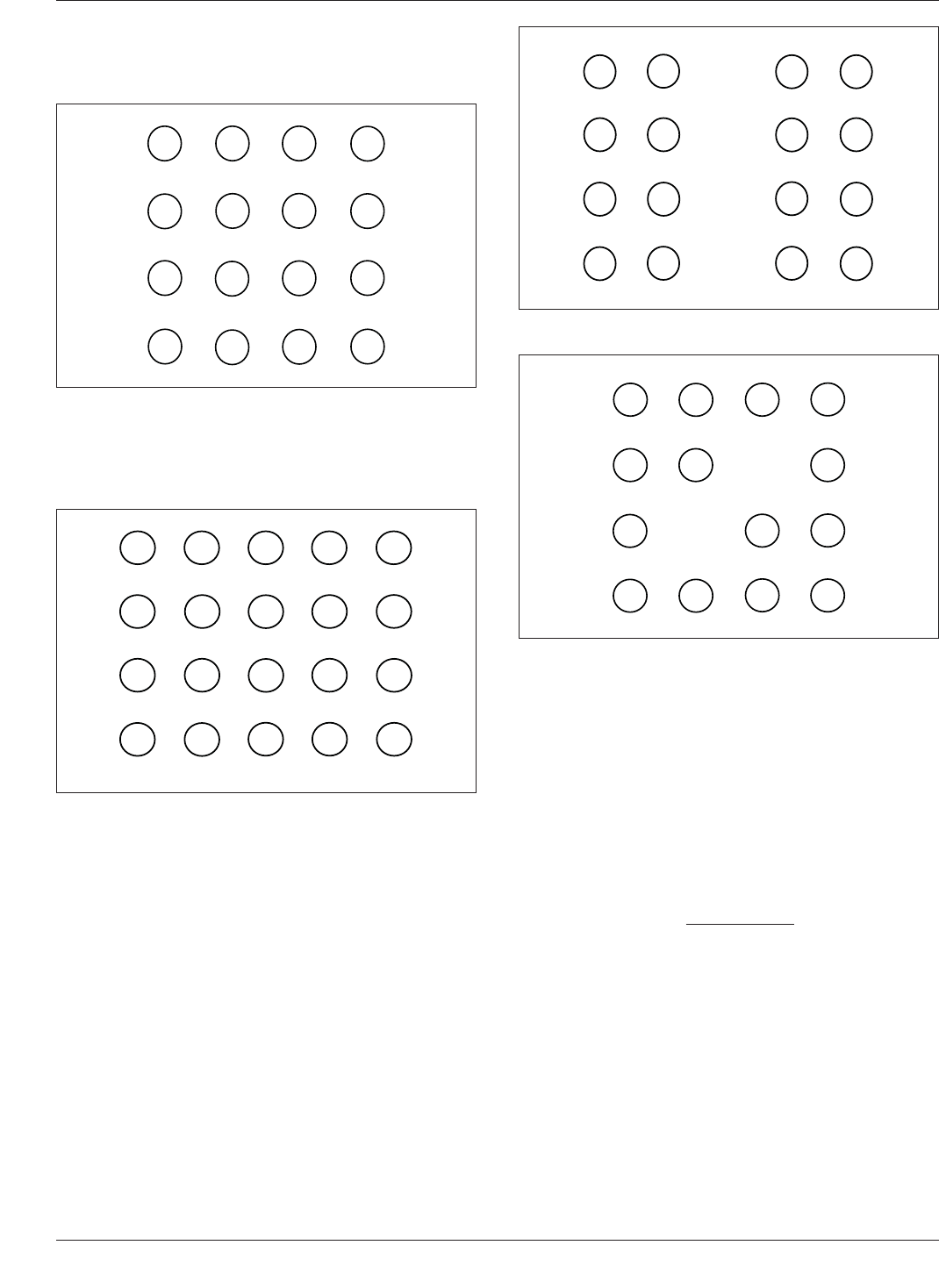
Ball grid arrays can be square or can be rectangular. In a
square array, the number of rows is equal to the number of
columns. A 4x4 square array is shown in Figure 6-9.
In a rectangular array, the number of rows is not equal to
the number of columns. A 4x5 rectangular array is shown
in Figure 6-10.
The arrays may be completely filled or certain portions of
the array may be unfilled. A 4x5 rectangular array is shown
in Figure 6-11 which has one central column unused,
blank, or depopulated.
The 4x4 square array shown in Figure 6-12 has some balls
missing, blank or depopulated.
It is relatively trivial to fan out the conductors from the
outlying balls to the periphery for interconnection to the
outside world. But the solder balls inside the array have to
be routed in between the outlying solder balls.
As the size of the array increases, more and more conduc-
tors from the solder balls inside the array have to be routed
in between the solder balls to connect to the outside world.
It is important for the substrate designers to know how
many conductors they may expect to accommodate in the
spacing between the adjacent solder balls so that they may
determine the widths of the conductors and the spacing
between the conductors. This information will help to
model the signal integrity to assure the success of their
application.
The number of conductors per outlet, C, for a simplerxc
array can be determined by substituting r and c in the fol-
lowing relationship with the number of rows and columns
of the given array, and by substituting d with the number
of depopulated sites in the array.
C
[(r−2)(c−2)]−d
2(r+c−2)
In case the above equation provides a whole number for C,
every array outlet between adjacent solder balls will need
to accommodate C conductors. If C is a fractional number
then some outlets will have to accommodate a number of
conductors obtained by rounding down the value of C, and
others will have to accommodate a number of conductors
obtained by rounding up the value of C. The fraction is the
proportion of the lower and higher number of conductors
per outlet.
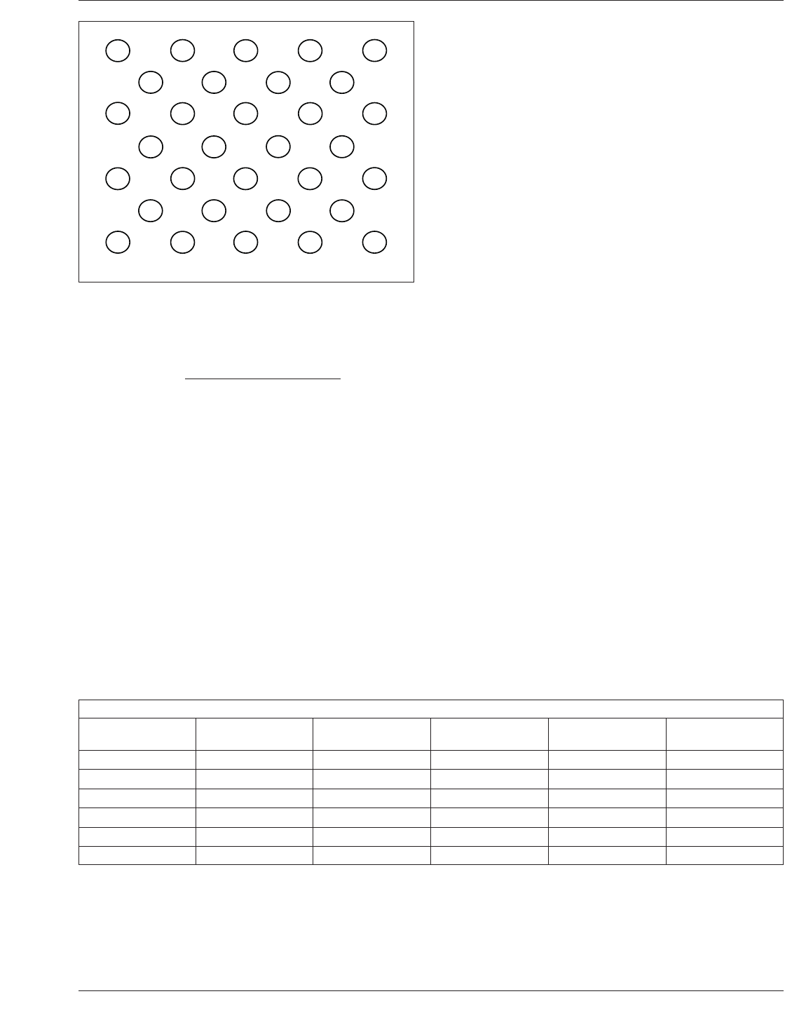
The balls in an array can also be interspersed, as in a
diagonal array. An example of a 5x5 interspersed array is
shown in Figure 6-13.
IPC-7095c-6-9
Figure 6-9 Square Array
IPC-7095c-6-10
Figure 6-10 Rectangular Array
IPC-7095c-6-11
Figure 6-11 Depopulated Array
IPC-7095c-6-12
Figure 6-12 Square Array with Missing Balls
IPC-7095C January 2013
56
Copyright IPC-Association Connecting Electronics Industries
Provided by IHS under license with IPC
Not for Resale
No reproduction or networking permitted without license from IHS
--`,,```,,,,````-`-`,,`,,`,`,,`---
The following relationship can be used to determine the
number of conductors per outlet for an interspersed array.
C =
[(r−2)(c−2)+(r−1)(c−1)]−d
2(r+c−2)
If C turns out to be a fraction, then rounding it down will
give the lower number of conductors to be accommodated
between some adjacent balls, and rounding it up will pro-
vide the number of maximum conductors needed to be
accommodated between other adjacent balls. The fraction
gives the proportion of the two numbers.
The sizes of the solder land and via land also affect the
routing ability of BGA packages. A 0.8 mm solder land on
a 1.27 mm pitch leaves only 0.5 mm between solder lands
for routing. In order to get two conductors between the
solder lands, 100/100 µm conductors/spacing would need
to be used. However, if a 0.6 mm solder land is used, two
conductors can be routed between lands using 125/125 µm
conductors/spacing.
Because of the small space between solder lands on finer
pitch BGA (1.00 mm and less), smaller via lands and drill
sizes are required. As the drill sizes get smaller, the maxi-
mum allowable board thickness also decreases. This may
force board designers to use fewer layers or to decrease the
dielectric thickness between layers.
If microvias are used, this may force the outer two layers
of the PCB to be signal layers.
6.3.1 Escape Strategies Table 6-4 shows some escape
strategies for full arrays.
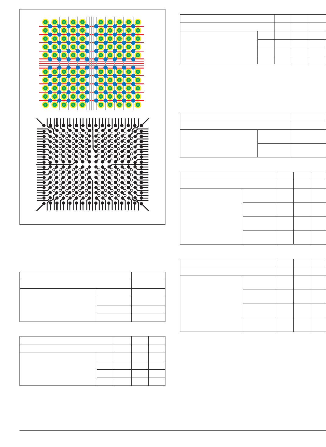
To accommodate a flip chip with area array I/O lands at
0.25 mm pitch, the BGA package substrate will need bond-
ing lands at 0.25 mm pitch on the top side, and solder balls
at 1.27 or 1.00 mm pitch on the bottom side. These oppos-
ing sets of lands must be connected by the BGA package
substrate (high-density microcircuit board) wiring and
interlevel vias or PTHs. It may be necessary to have one or
more interconnecting lines between two adjacent bonding
lands on the topside of the BGA substrate. This is done in
order to access multiple rows of the interior I/O lands for
connection to the vias or PTHs for eventual connection to
the solder balls on the bottom side. Very aggressive layout
rules must be used, even when designing with surface
redistribution layers (see Figure 6-14).
For high performance chips with 1700 pin requirements,
a BGA with very dense wiring layers is required. The body
size of such a BGA would be 50 mm. In all probability,
there would be depopulated solder balls in the middle
of the BGA. Regarding pitch, such a BGA substrate
would require a 1.00 mm via and solder ball pitch, which
would accommodate a ball density of 100 I/O per square
centimeter.
IPC-7095c-6-13
Figure 6-13 Interspersed Array
Table 6-4 Escape Strategies for Full Arrays
Full array parts
Pitch (mm)
Nominal Ball
Diameter (mm) Surface Traces
Dog Bone
Through Vias
Dog Bone
Microvias Microvia in Pad
1.27 0.75 Y Y Y Y
1.0 0.45 - 0.6 Y Y Y Y
0.8 0.3 - 0.5 Y Y Y Y
0.75 0.3 - 0.45 N H, S Y Y
0.65 0.3 - 0.4 N N Y Y
0.5 0.3 N N N Y
Notes:
See Table 6-5 to 6-7 for details on routing channel widths
See Tables 6-8 to 6-10 via drill and land size assumptions used
Y = yes, with ‘‘standard’’ board fabrication capability and standard land size
H = high capability board fabrication required
S = shrink land size required
N = not practical with industry standard design & process
January 2013 IPC-7095C
57
Copyright IPC-Association Connecting Electronics Industries
Provided by IHS under license with IPC
Not for Resale
No reproduction or networking permitted without license from IHS
--`,,```,,,,````-`-`,,`,,`,`,,`---
6.3.2 Surface Conductor Details Tables 6-5 through 6-7
shows various conductor routing characteristics for differ-
ent BGA pitches.
6.3.3 Dog Bone Through Via Details Tables 6-8 through
6-10 provide the details for conductor routing using the
dogbone via concept. The tables also are organized per via
pitch.
6.3.4 Design for Mechanical Strain Mechanical strain
and board flexure are major causes of PCB and BGA joint
damage. Several BGA layout strategies have been devel-
oped that can help reduce the impact of mechanical strain
on the BGA.
IPC-7095c-6-14
Figure 6-14 Conductor Routing Strategy
Table 6-5 Conductor Routing - 1.27 mm Pitch
Nominal Ball Diameter (mm) 0.75
Typical Solder Land Diameter (mm) 0.55
Conductor Spacing Width (µm) 150 2
125 2
100 3
75 4
Table 6-6 Conductor Routing - 1.0 mm Pitch
Nominal Ball Diameter (mm) 0.6 0.5 0.45
Typical Solder Land Diameter (mm) 0.45 0.40 0.35
Conductor Spacing Width (µm) 150 1 1 1
125 1 1 2
100 2 2 2
75333
Table 6-7 Conductor Routing - 0.8 mm Pitch
Nominal Ball Diameter (mm) 0.45 0.4 0.3
Typical Solder Land Diameter (mm) 0.35 0.3 0.25
Conductor Spacing Width (µm) 150 1 1 1
125 1 1 1
100 1 2 2
75123
Table 6-8 Conductor Routing - 1.27 mm Pitch
Nominal Ball Diameter (mm) 0.75
Typical Solder Land Diameter (mm) 0.55
Drill Diameter 0.35 mm
[0.0135 in]
Y
0.3 mm
[0.012 in]
Y
Table 6-9 Conductor Routing - 1.0 mm Pitch
Nominal Ball Diameter (mm) 0.6 0.5 0.45
Typical Solder Land Diameter (mm) 0.45 0.40 0.35
Drill Diameter 0.35 mm
[0.0135 in]
NNY
0.3 mm
[0.012 in]
NYY
0.25 mm
[0.010 in]
YYY
0.2 mm
[0.008 in]
YYY
Table 6-10 Conductor Routing - 0.8 mm Pitch
Nominal Ball Diameter (mm) 0.45 0.4 0.3
Typical Solder Land Diameter (mm) 0.35 0.3 0.25
Drill Diameter 0.35 mm
[0.0135 in]
NNN
0.3 mm
[0.012 in]
NNN
0.25 mm
[0.010 in]
NYY
0.2 mm
[0.008 in]
YYY
IPC-7095C January 2013
58
Copyright IPC-Association Connecting Electronics Industries
Provided by IHS under license with IPC
Not for Resale
No reproduction or networking permitted without license from IHS
--`,,```,,,,````-`-`,,`,,`,`,,`---