IPC-7095C-2013.pdf - 第136页
higher melting point. Some component manufacturers have had unexpected yield losses due to low Ag alloys when they were not aware of their presence. The change to low Ag ball alloys may require a change to the PCA reflow …

8.2.2 Mixed Alloy Soldering During the transition to
lead-free reflow soldering, there will be occasions when it
may be necessary to solder tin/lead and lead-free BGAs on
the same PCBA with tin/lead or lead-free solder. Soldering
mixed alloy BGAs is an undesirable scenario, but it is
likely to happen. The most likely scenario is soldering
lead-free BGAs with tin/lead solder. This scenario occurs
when a component supplier provides end-of-life (EOL) tin/
lead BGAs in favor of lead-free BGAs. When confronted
with this situation there are several options:
• Refuse to build the PCBA
• Reball the BGA with tin/lead solder balls (may not be
acceptable to all companies)
• Convince the supplier to provide a Sn/Pb version
8.2.2.1 Reflow Solder Using a Lead-Free Profile Some
companies have successfully soldered mixed alloy BGAs
and the reliability results have been acceptable in many
cases. Studies have shown that the homogeneous contami-
nation of SAC solder with <20% wt. Lead will not degrade
fatigue life below that of tin/lead. However, be very cau-
tious. Perform adequate reliability testing (cross-sections,
thermal cycling, shock testing) to confirm solder joint reli-
ability in the intended use environment.
All components on a mixed alloy (lead-free BGAs with
tin/lead solder) PCBA should be evaluated for lead-free
soldering process compatibility before soldering is
attempted. This evaluation will ensure that all components
will survive lead-free soldering temperatures. While most
tin/lead components are rated to a peak temperature of
230°C, evidence suggests that many tin/lead components
will survive lead-free soldering temperatures, though this is
not always the case. Once again, be very cautious.
Adequate reliability testing should be done to confirm reli-
ability expectations. Use Table 8-1 as a guide for compo-
nent compatibility with lead-free soldering process tem-
peratures.
8.2.2.2 Reflow Solder Using a Tin/Lead Profile When
the assembly comprises both lead-free SAC BGAs and tin/
lead BGAs and/or when the PCBA has not converted to a
lead-free system or is not required to be a lead-free system,
such as the RoHS exempted industry sectors/applications, a
tin/lead eutectic paste continues to be used.
Under such scenarios, a tin/lead eutectic reflow profile hav-
ing the adequate peak temperature, dwell time and proper
preheat must be used. More details about such scenarios
are contained in Section 7.
8.2.2.3 Implementation of BGAs with Low-Ag SAC, or
doped SAC, and Non-SAC BGA Ball Alloys
During the
initial lead-free transition, the BGA solder ball alloys used
typically matched the assembly process alloys of
Sn96.5Ag3.0Cu0.5 (SAC305), Sn95.5Ag3.8Cu0.7
(SAC387) or Sn95.5Ag4.0Cu0.5 (SAC405). Problems such
as balls dropping off and susceptibility to mechanical shock
and thermally-induced strains have led BGA suppliers to
evaluate and suggest the use of additional alloys for the
balls. For some packages, the change involves moving
from silver (Ag) content of 3-4% down to 1-3%. Depend-
ing on the specific Ag content, the reduced Ag content will
increase the melting point of the solder ball by as much as
10°C. This can have a significantly adverse impact on the
PCBA assembly process. Great care must to be taken when
introducing new alloys into BGAs and new alloyed BGAs
into the assembly process.
The addition of doping elements to SAC system have also
been studied, offering improvements in some aspects of
mechanical properties. However, these additions largely do
not change the physical properties, particularly do not
lower the melting temperature of the alloy. Some doping
elements may affect solder under-cooling, the formation of
Intermetallic, matrix properties, Other non-SAC alloys, by
taking an entirely different metallurgical approach, offer
lower melting temperature, thus substantially favorable
assembly process and better mechanical properties from
reliability point view. But these alloys are more costly in
raw materials.
8.2.2.4 PCA Manufacturing Impact of Pb-Free The new
lead-free BGA ball alloys may have an impact on the
printed circuit assembly (PCA) reflow process due to
Table 8-1 Tin/Lead Component Compatibility with Lead-Free Reflow Soldering
Tin/lead Component Type Compatibility
Ceramic resistors/capacitors Okay
Molded capacitors (tantalum) Use lead-free process temperature compatible components only
Aluminum electrolytic capacitors Use lead-free process temperature compatible components only
Molded ICs (SO, PLCC, QFP) Use lead-free process temperature compatible components only
Connectors, sockets, etc. Use lead-free process temperature compatible components only
Crystals, oscillators Use lead-free process temperature compatible components only
Transistors, diodes Okay
LEDs Use lead-free process temperature compatible components only
BGAs May or may not be Okay. Evaluate on a case-by-case basis
DIP switches Okay
January 2013 IPC-7095C
121
Copyright IPC-Association Connecting Electronics Industries
Provided by IHS under license with IPC
Not for Resale
No reproduction or networking permitted without license from IHS
--`,,```,,,,````-`-`,,`,,`,`,,`---
higher melting point. Some component manufacturers have
had unexpected yield losses due to low Ag alloys when
they were not aware of their presence. The change to low
Ag ball alloys may require a change to the PCA reflow tar-
get temperatures. For example, an increase of 10°C in
melting point for a specific BGA may cause other locations
on the PCA to exceed the temperature limits of either com-
ponents or PCB.
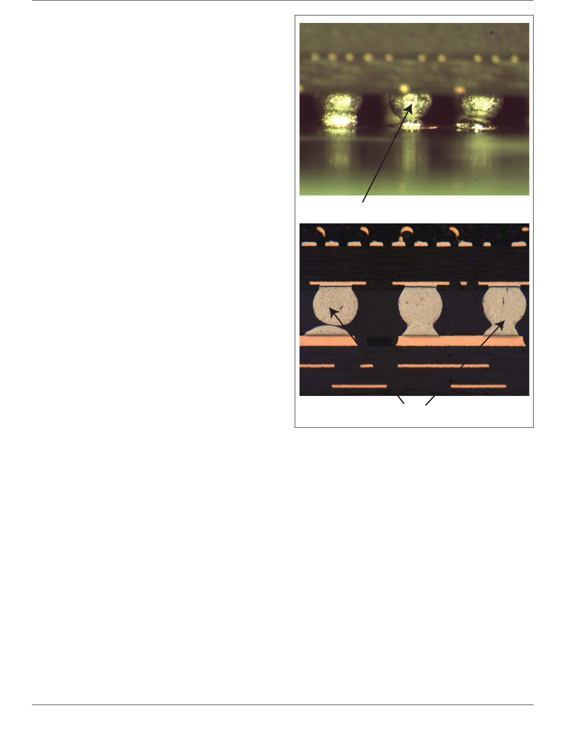
Reliability Impact – Improperly assembled low Ag parts,
assembled with too low of a reflow temperature, are at sig-
nificant reliability risk since they may pass electrical test
but may still produce an unacceptable solder joint (see Fig-
ure 8-5). Some experimental data suggests that the drop
performance of well manufactured low Ag parts are better
than current SAC alloys, such as SAC305, SAC405 and
SAC387; however, the fatigue life of low Ag alloys is con-
sistently lower than their Ag counterparts. Additional fac-
tors (BGA pad and PCB land finish) are critical for reliabil-
ity and are being investigated.
8.3 Solder Joints and Attachment Types Solder joints
are not homogeneous structures. A solder joint consists of
a number of different materials, many of which are only
superficially characterized. A solder joint consists of:
1) The base metal at the printed board.
2) One or more intermetallic compounds (IMC).
3) The bulk solder.
4) A layer from which the solder constituent forming the
component-side IMC(s) has been depleted.
5) One or more IMC layers of a solder constituent with
the component base metal.
6) The base metal at the component.
The grain structure of solder continues to change over time.
At room temperature, eutectic tin/lead solder is above its
recrystallization temperature; the grains will grow in size
over time. The grain structure growth reduces the internal
energy of a fine-grained structure. This grain growth pro-
cess is enhanced by elevated temperatures as well as strain
energy input during cyclic loading. The grain growth pro-
cess is thus, to some degree, an indication of the accumu-
lating fatigue damage. This indication is significantly more
pronounced for solder joints subjected to aging (and is less
pronounced in cyclic testing) than for solder joints in
operational use. Contaminants, like tin oxides and flux resi-
dues, sometimes migrate to the outer surface of the solder,
but reside predominantly at the grain boundaries. As the
grains grow, the concentration of these contaminants is
increased at these grain boundaries, therefore weakening
the solder. After the consumption of about 25% of the
fatigue life of the solder, micro-voids can be found at the
grain boundary intersections; these micro-voids grow into
micro-cracks after 40% of the fatigue life. These micro-
cracks grow and coalesce into macro-cracks leading to total
fracture of the solder joint.
The solder joints frequently connect materials of differing
properties, one of which is global thermal expansion mis-
match. Solder often has properties significantly different
than the bonding structure materials, causing local thermal
expansion mismatches. The severity of these thermal
expansion mismatches, and thus the severity of the reliabil-
ity threat, depends on the design parameters of the assem-
bly and the operational use environment. For lead-free sol-
der joints, there is a higher propensity for differential solid
diffusion causing Kirkendall voids, also known as IMC
Microvoids. The higher propensity for IMC microvoiding
is associated, at least in part, with the higher soldering
temperatures required for lead-free solders. Further, Planar
Microvoiding is seen on lead-free surface finishes such as
Immersion Silver, which entail typically more complex sol-
dering surface treatments than HASL.
IPC-7095c-8-5
Figure 8-5 Incomplete Solder Joint Formation for 1% Ag
Ball Alloy Assembled at Low End of Typical Process Window
Unmelted solder ball
CSP Package
PCB
CSP Package
PCB
Unacceptable solder joints
IPC-7095C January 2013
122
Copyright IPC-Association Connecting Electronics Industries
Provided by IHS under license with IPC
Not for Resale
No reproduction or networking permitted without license from IHS
--`,,```,,,,````-`-`,,`,,`,`,,`---
8.3.1 Global Expansion Mismatch The global expansion
mismatches result from differential thermal expansions of
an electronic component or connector and the printed board
to which it is attached via the surface mount solder joints.
These thermal expansion differences result from differences
in the CTEs and thermal gradients as the result of thermal
energy being dissipated within active components. Global
CTE mismatches typically range from about 2 ppm/°C for
CTE-tailored high reliability assemblies to ≥14 ppm/°C for
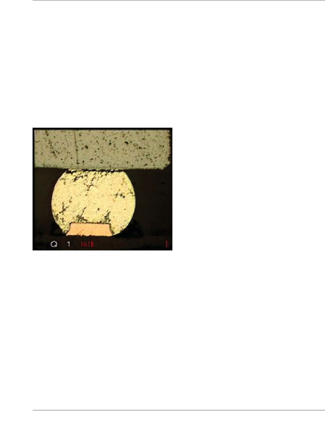
ceramic components on FR-4 printed boards. Figure 8-6 is
showing a solder joint failure due to CTE mismatch on a
wafer level CSP. The silicon die on the top expands much
less than the FR-4 substrate on the bottom. This causes
shear stress on the solder joint, which eventually fails at the
die to solder interface when subjected to temperature
cycling stresses.
8.3.2 Local Expansion Mismatch The local expansion
mismatch results from differential thermal expansions of
the solder and the base material of the component or PWB
to which it is soldered. These thermal expansion differ-
ences result from differences in the CTE of the solder and
those of the base materials from thermal excursions. Local
CTE mismatches typically range from 7 ppm/°C with cop-
per to 18 ppm/°C with ceramic and 20 ppm/°C with Alloy
42 and Kovar. Local thermal expansion mismatches typi-
cally are smaller than the global expansion mismatches,
since the acting distance, the maximum wetted area dimen-
sion, is much smaller: in the order of hundreds of microm-
eters instead of thousands.
8.3.3 Internal Expansion Mismatch In tin/lead solders,
an internal CTE mismatch results from the different CTEs
of the tin-rich and lead-rich phases of the solder. Internal
thermal expansion mismatches typically are the smallest,
since the acting distance, the size of the grain structure, is
much smaller than either the wetted length or the compo-
nent dimension - in the order of less than 25 µm.
For lead-free solders, the metallurgy is more complicated
due to the ternary or quarternary alloy composition concen-
trated at very high tin contents.
8.4 Solder Attachment Failure Failure of the solder
attachment of a component to the substrate to which it is
surface mounted is commonly defined as the first complete
fracture of any of the solder joints of which the component
solder attachment consists. Given that the loading of the
solder joints is typically in shear, rather than in tension, the
mechanical failure of a solder joint is not necessarily the
same as the electrical failure. Electrically, the mechanical
failure of a solder joint results, at least initially, in the
occasional occurrence of a short-duration (<1 µs) high
impedance event during either a mechanical or thermal dis-
turbance.
From a practical point of view, the solder joint failure is
defined as the first observation of such an event. For some
applications this failure definition might be inadequate. For
high speed signals with sharp rise times, signal deteriora-
tion prior to the complete mechanical failure of a solder
joint might require a more stringent failure definition.
Similarly, for applications which subject the electronic
assemblies to significant mechanical vibration and/or shock
loading, a failure definition that considers the mechanical
weakening of the solder joints as the result of the accumu-
lating fatigue damage might be necessary.
8.4.1 Solder Attachment Failure Classification There
are some common BGA failure signatures. These defects
can be induced during the assembly process or they could
be latent solder joint defects or failures. Such defects
and/or failures are the result of an inadequate assembly
process, defective material or excessive mechanical stress
during assembly. The defects could be a partial open or
very weak interfaces, the latent failures could be hairline
cracks, open joint with a full contact and partially lifted
land. They are difficult to detect using conventional process
verification tools such as X-ray and ICT test. They are a
major reliability concern since they can be intermittent.
Subsequently, they are tracked down following high levels
of fields returns.
8.4.2 Failure Signature-1: Cold Solder Cold solder joint
is a result of a low peak temperature during the reflow pro-
cess (<Liquidus+20°C). The Liquidus temperature of a sol-
der alloy is the temperature above which the whole solder
volume is liquid. The solder paste partially melts and will
form a cold solder joint. The joint may have a rough sur-
face and sometimes necking at the interface to the board.
The solder will appear grainy as shown in Figure 8-7 and
there will be a difference between the grain structure of the
Figure 8-6 Solder Joint Failure Due to Silicon and Board
CTE Mismatch
January 2013 IPC-7095C
123
Copyright IPC-Association Connecting Electronics Industries
Provided by IHS under license with IPC
Not for Resale
No reproduction or networking permitted without license from IHS
--`,,```,,,,````-`-`,,`,,`,`,,`---