IPC-7095C-2013.pdf - 第153页
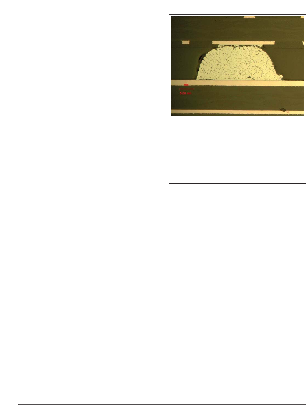
9.1.2 Solder Mask Defined Land on Product Board The main disadvantage of solder mask defined land is that the stress concentrations created by SMD (solder mask defined) solder joint can be the origin of solder joint fail- …
9 DEFECT AND FAILURE ANALYSIS CASE STUDIES
The following clauses identify possible assembly anoma-
lies related to the assembly of BGA components. The
descriptions include post process failures related to the
mounting structure characteristics and the variation in the
solder ball used as the BGA termination. In many instances
attachment metallurgy are discussed especially if the char-
acteristics contributed to the joint failure. Final joint con-
figurations are also analyzed.
9.1 Solder Mask Defined BGA Conditions There are
two ways BGA Lands are defined: solder masked defined
(SMD) where the land size is larger than solder mask and
the molten BGA ball touches the solder mask after reflow.
The other method for designing the BGA land is called
etched or nonsolder mask defined (NSMD) where the mask
opening is larger than the copper land and hence the ball
does not touch the solder mask after reflow. This condition
is shown in 9.1.1 and 9.1.2.
Solder mask-defined lands may be used on corresponding
noncritical or functional pins, since SMD lands can help
minimize pad cratering defects. However, it should be
understood that solder mask defined lands create additional
stress initiation sites and should be avoided on both the
interposer and the printed board land.
9.1.1 Solder Mask Defined and Nondefined Lands
Possible Cause
Interposer is solder mask defined; board is metal-defined. If the
two areas are very different, the stresses are not uniform and
cracks may occur at the solder mask defined side. Board land
pattern too large.
Potential Solution
Area of the two attachment conditions should be similar or
identical. In addition, solder mask defined lands create addi-
tional stress initiation sites and should be avoided on both the
interposer and the printed board land.
IPC-7095C January 2013
138
Copyright IPC-Association Connecting Electronics Industries
Provided by IHS under license with IPC
Not for Resale
No reproduction or networking permitted without license from IHS
--`,,```,,,,````-`-`,,`,,`,`,,`---
9.1.2 Solder Mask Defined Land on Product Board
The main disadvantage of solder mask defined land is that
the stress concentrations created by SMD (solder mask
defined) solder joint can be the origin of solder joint fail-
ures and reduced reliability. This condition is shown in
9.1.3. For equal solder joint height, increases in fatigue life
by factors of about 1.25 to 3 can be anticipated with the
use of nonsolder mask defined (NSMD) vs. SMD lands,
with the larger improvements for solder joints with the
more severe loading conditions.
There are three main disadvantages of SMD lands:
• Less real estate for topside breakout
• Loss of accuracy of land dimension
• Reduced reliability as it is the origin of early solder joint
failure
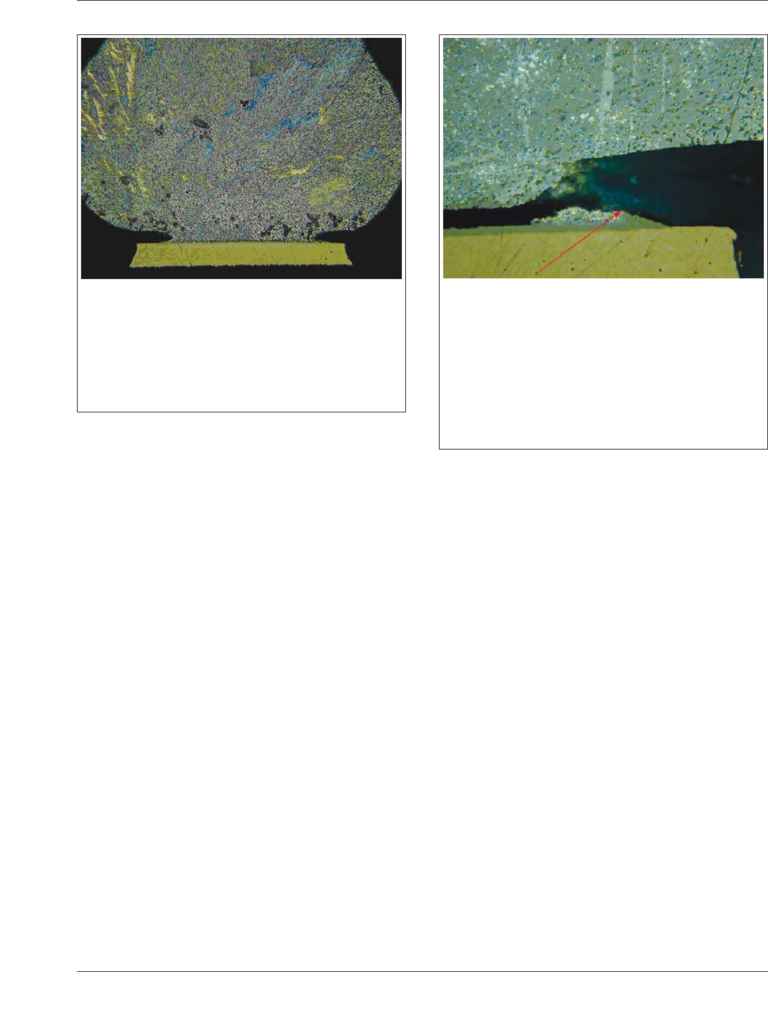
9.1.3 Solder Mask Defined BGA Failures
Possible Cause
Solder mask encroaches too far on land at board level. This
condition creates stresses in the ball that can propagate a
crack during temperature changes.
Potential Solution
Always design product boards using only metal-defined
(NSMD) lands, unless a solder mask defined land is needed to
reduce the incidence of pad cratering.
Crack starts in the solder and eventually travels down to
and through the intermetallic layer. Nickel buildup under
the solder mask is also evident.
Possible Cause
Crack starts in solder at sharp corner of solder mask. The con-
dition due to stresses in the ball caused crack propagation.
Potential Solution
Always design product boards using only metal-defined
(NSMD) lands, unless a solder mask defined land is needed to
reduce the incidence of pad cratering.
January 2013 IPC-7095C
139
Copyright IPC-Association Connecting Electronics Industries
Provided by IHS under license with IPC
Not for Resale
No reproduction or networking permitted without license from IHS
--`,,```,,,,````-`-`,,`,,`,`,,`---
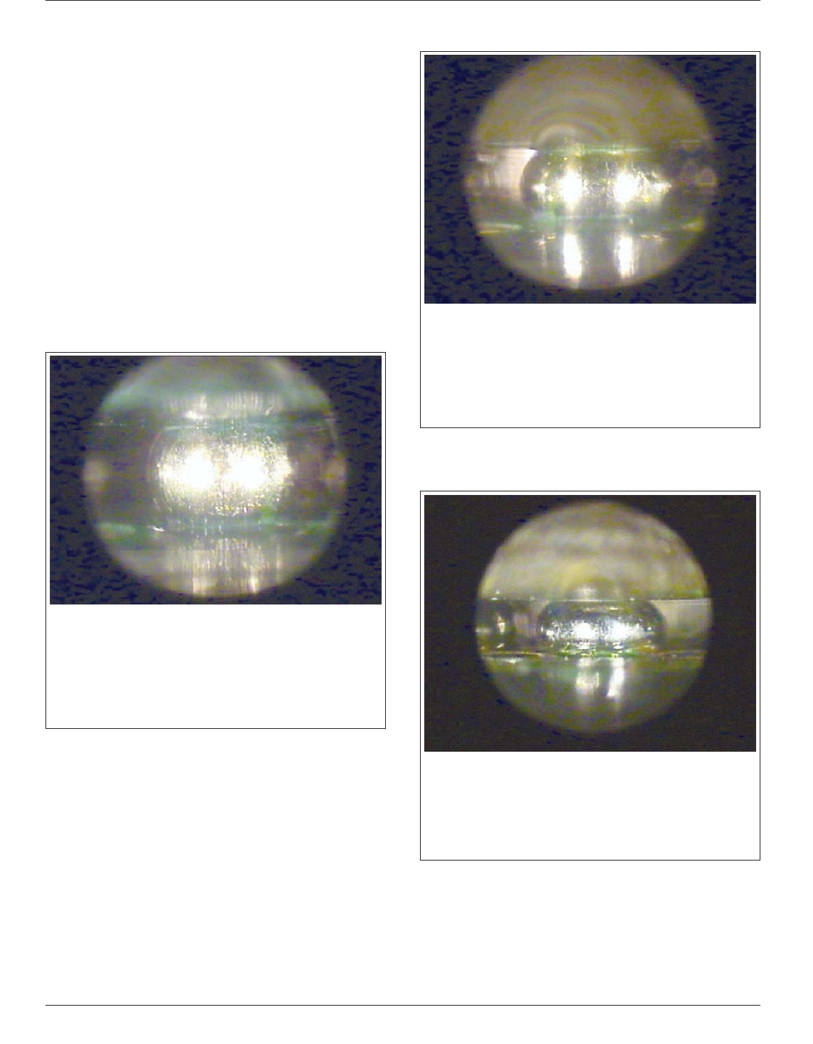
9.2 Over-Collapse BGA Solder Ball Conditions The
plastic BGA, generally, has solder balls that collapse to
about 625 µm from its original size of 750 µm. After the
package is soldered to the board, the ball collapses to about
500 µm. However, if there is a heat spreader or a heat slug
in the package for heat dissipation, the ball may collapse to
as low as 300 µm. As the ball flattens there is a decrease in
reliability due to limited solder height and solder joint
compliancy. Also, solder ball spread may occur beyond the
desirable pitch clearance. A good approximation is that the
initial reflow reduces the height by about 10%; with the
added weight of a heat spreader this figure may increase to
25% of the original height (ball diameter). The land pattern
and solder mask clearance also play a part in the analysis.
The extremes of this condition are shown in 9.2.1 through
9.2.4.
9.2.1 BGA Ball Shape without Heat Slug 500 µm Stand-
off Height
9.2.2 BGA Ball Shape with Heat Slug 375 µm Standoff
Height
9.2.3 BGA Ball Shape with Heat Slug 300 µm Standoff
Height
Possible Cause
Weight of BGA does not over-collapse ball. This is the target
condition and becomes the measure of evaluation over other
BGAs or balls on the same BGA.
Potential Solution
Use spacer if more clearance is desired. It should also be
judged to check on the variation between ball collapse.
Possible Cause
Weight of BGA with heat slug causes ball to over-collapse. This
deformation may be acceptable depending on the component
pitch so that balls do not touch.
Potential Solution
Mandatory requirement to include spacer preventing ball col-
lapse.
Possible Cause
Weight of BGA with heat slug causes ball to over-collapse. This
is a definite poor quality condition and should be remedied.
Potential Solution
Mandatory requirement to include spacer preventing ball col-
lapse.
IPC-7095C January 2013
140
Copyright IPC-Association Connecting Electronics Industries
Provided by IHS under license with IPC
Not for Resale
No reproduction or networking permitted without license from IHS
--`,,```,,,,````-`-`,,`,,`,`,,`---