IPC-7095C-2013.pdf - 第96页
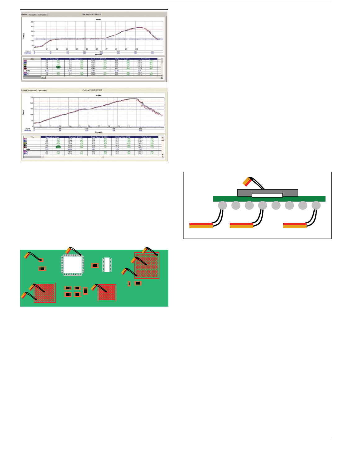
7.1.4.5 Thermocouple Attachment Figure 7-8 shows recommended locations of thermocouples on a board. It is important that thermocouples be attached onto small and large components at the solder joints. For BGAs, it is als…
board between 210-220°C, one could easily get away by
maintaining temperature between 190-225°C, a variation of
almost 35°C and still achieve good reflow soldering results.
In lead-free assembly, the commonly used SAC (Sn, Ag,
and Cu) solders contain 3 to 4% silver, 0.5 to 0.7% copper
and the rest tin. These alloys have the melting point around
220°C. A few components, such as some aluminum elec-
trolytic capacitors, put restrictions on maximum tempera-
ture and duration above 230°C to which they can be sub-
jected. Additional constraints will be dictated by low cost
laminates, plastic connectors and moisture sensitive com-
ponents if used.
To accommodate such constraints, the peak temperature in
lead-free assemblies should be maintained between 230-
245°C, a variation of only 15°C—a tight process window
indeed. This is about a 60% drop from 35°C variation
within tin/lead assemblies as mentioned earlier. The diffi-
culty of achieving a reflow profile to meet the defined pro-
cess window is further increased if large components with
high thermal mass are used on the same board with smaller,
temperature sensitive components. The reasons are simple.
The large components with high thermal mass require a
larger heat input to meet the process window requirements
for Peak Temperature and time above liquidus. However,
this large heat input may result in the smaller, temperature
sensitive components falling outside the process window
requirements. To resolve this issue, very tight process con-
trol and narrow temperature bandwidth across the board is
necessary. Many assembly houses may have a hard time
meeting such requirements, especially on complex boards
without concerted time and effort in developing reflow pro-
files.
The problem can be further compounded by backward
compatibility issues where some lead-free components are
used on a primarily tin/lead board. In such cases, the pro-
file must accommodate both tin/lead and lead-free package
requirements.
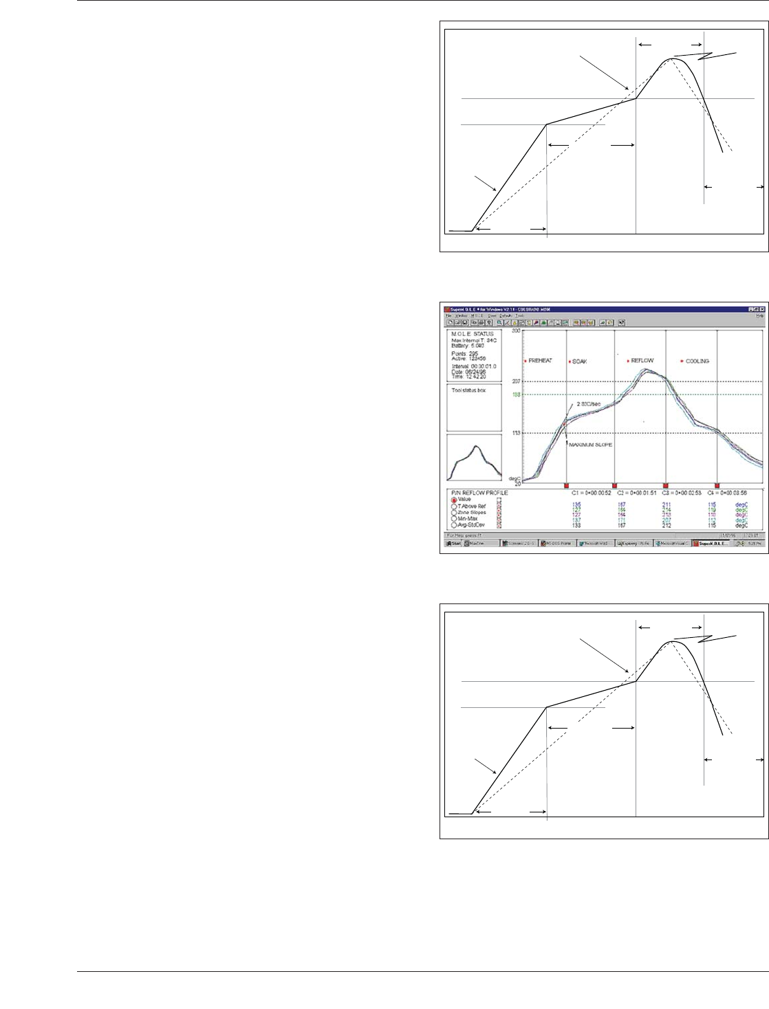
Figures 7-4 to 7-7 show schematic and actual profiles for
tin/lead, lead free, and assemblies with tin/lead and lead-
free components.
7.1.4.4 Preheat Zone The temperature in the preheat
zone can range from 30-175°C and many component sup-
pliers generally recommend 2-4°C/second ramp rate to
avoid thermal shock to sensitive components. Such guide-
lines are considered conservative since some capacitors are
wave soldered where they go from preheat temperature of
about 120°C to wave pot temperature of 260°C. The fast
ramp rate does increase the potential for solder balls and
hence should be kept as low as feasible; however, consid-
eration should be given to the acceptable ramp rate of the
most sensitive component on the assembly.
IPC-7095c-7-4
Figure 7-4 Schematic of Reflow Profile for Tin/Lead
Assemblies
PREHEAT
SOAK
REFLOW
COOLING
210 to 220°C
183°C
Ramp to Peak Profile
with no Soak
100-180°C
Cool Down
4-8°C/Second
60-90 SEC
60-90 SEC
30-60 SEC
for cooling
to room temp
MAX SLOPE
OF 5°C/SEC
90-120 SEC
Figure 7-5 An Example of Tin/Lead Profile with Multiple
Thermocouples
IPC-7095c-7-6
Figure 7-6 Schematic of Reflow Profile for Lead-Free
Assemblies
PREHEAT
SOAK
REFLOW
COOLING
235 to 245°C
217°C
Ramp to Peak Profile
with no Soak
140-220°C
Cool Down
4-8°C/Second
60-90 SEC
60-90 SEC
30-60 SEC
for cooling
to room temp
MAX SLOPE
OF 5°C/SEC
90-120 SEC
January 2013 IPC-7095C
81
Copyright IPC-Association Connecting Electronics Industries
Provided by IHS under license with IPC
Not for Resale
No reproduction or networking permitted without license from IHS
--`,,```,,,,````-`-`,,`,,`,`,,`---
7.1.4.5 Thermocouple Attachment Figure 7-8 shows
recommended locations of thermocouples on a board. It is
important that thermocouples be attached onto small and
large components at the solder joints. For BGAs, it is also
important to attach a thermocouple at the top of the pack-
age.
In developing any profile, it is very important to use the
right thermocouple. Type k thermocouples with wire gauge
of 36 AWG should be used. Thicker thermocouple wires
add too much heat sink. Thermocouple wire length should
not exceed three feet for good accuracy. To ensure accu-
racy, thermocouple junctions must be welded. No twisting,
crimping or soldering should be used.
Care should be exercised when using high temperature
tapes such as polyimide (kapton®) or aluminum tapes.
Tapes tend to come loose during reflow and the system
measures the temperature of the air in the oven and not the
temperature of the solder joints. It is important to make
sure that there is good contact of the tape, otherwise, a high
temperature solder or thermally conductive adhesive
should be used to attach thermocouples to the solder joints.
One benefit with using tape is that the thermocouples can
be reused repeatedly without damaging them.
In the case of BGAs, drill holes in the center and corner
balls of the BGA from the bottom of the board and push
the thermocouples to the top to correctly measure the tem-
perature of BGA balls. It is important that the difference in
temperature of the center and corner balls of the same
BGA are within 2°C of each other. There are also some
thermocouples that can be inserted under the BGA, elimi-
nating the hole drilling process; however, in this instance,
the thermocouples may only be measuring the temperature
under the device.
Four to six thermocouples should be attached at various
component locations to represent the lowest to highest ther-
mal mass areas including at least two thermocouples for
BGAs. Figure 7-9 shows locations of thermocouples on a
BGA.
7.1.4.6 Soak Zone The soak zone is intended to bring
the temperature of the entire board up to a uniform
temperature. The ramp rate in this zone is very slow,
almost flat when raising the temperature from 75-220°C.
The soak zone also acts as the flux activation zone for sol-
der paste. The consequences of having too high a tempera-
ture in the soak zone are solder balls, solder splatter due to
excessive oxidation of paste, and spent flux activation
capability. The purpose of long soak zone is to minimize
voids, especially in BGAs. It is also common practice not
to use soak zone but to steadily ramp the temperature from
preheat zone to peak reflow. However, the likelihood of
voids may be increased when ramping steadily to peak
reflow temperature.
7.1.4.7 Reflow Zone The peak temperature in the reflow
zone should be high enough to obtain good wetting, and
create a strong metallurgical bond. However, it should not
be so high as to cause component or board damage or dis-
coloration or, in worst case, charring of the board. If the
temperature is too low, cold and grainy solder joints, non
melted solder, or poor inter-metallic bonding may result.
As shown in Table 7-3, the peak temperature in this zone
Figure 7-7 Examples of Lead-Free Profiles with Soak (Top)
and Ramp to Peak (Bottom) with Multiple Thermocouples.
The Profiles with Soak Tend to Reduce Voids in BGAs.
Figure 7-8 Locations of Thermocouples on a Board with
Large and Small Components
IPC-7095c-7-9
Figure 7-9 Recommended Locations of Thermocouples
on a BGA
IPC-7095C January 2013
82
Copyright IPC-Association Connecting Electronics Industries
Provided by IHS under license with IPC
Not for Resale
No reproduction or networking permitted without license from IHS
--`,,```,,,,````-`-`,,`,,`,`,,`---

should be maintained between 230-245°C for lead-free.
The time above liquidus (TAL) should be 60 to 90 seconds.
Extended duration above the solder melting point or TAL
will damage temperature sensitive components. It also
results in excessive intermetallic growth which makes the
solder joint brittle and reduces solder joint fatigue resis-
tance.
7.1.4.8 Cooling Zone The typical cooling rate for most
assemblies has been 4-6°C per second, driven primarily by
throughput and SnPb intermetallic thickness concerns.
With the transition to Pb-free solders, the pad cratering
defect has become more common due to the increased stiff-
ness of the SAC solders and the reduction in the flexure
resistance of laminates. Pad cratering has been identified
directly after the reflow process leading to several experi-
ments designed to understand the impact of cooling rate.
During the cooling phase, the various materials in the
y-axis of a solder joint will cool at different rates. Typically
the BGA package will cool faster than the solder joint and
much faster than the PCB. This differential cooling can
create mechanical strain on the weakest spot in the
interconnect, the laminate below the BGA pad. By slowing
the cooling rate significantly, to as low as 1.5°C per sec-
ond, all of the materials in the y-axis will cool more slowly
and will reduce the strain placed on the laminate. Experi-
mental work performed by consortia has shown that this
slowed cooling does not appear to negatively impact the
solder joint intermetallics nor the grain structure of the
joint. If pad cratering is found immediately after reflow or
if the assembly is determined to be at risk for cratering,
then the cooling rate of the PCA should be slowed to
reduce strain.
7.1.4.9 Thermal Profile for Backward Compatibility
Developing a reflow profile is made difficult when dealing
with backward compatibility issues where some lead-free
components are used on a primarily tin/lead board. Back-
ward compatibility is a scenario where some components
are available only with lead-free surface finishes. Such a
scenario arises since it may not be economical for many
component suppliers to supply both tin/lead and lead-free
versions of the same component. It is not an issue when
using leaded components such as small outline integrated
circuit (SOIC), plastic leaded chip carrier (PLCC) or fine
pitch with lead-free surface finishes. Most tin/lead compo-
nents primarily have 85% tin surface finish with about 15%
lead. When component manufacturers eliminated the lead
from parts they plated pure tin; however, the solderability
suffered. To correct this condition, up to 5% bismuth was
added to the plating alloy to improve the wetting or solder-
ability to the part.
The real problem arises when using lead-free BGAs on a
primarily tin/lead board. If the tin/lead profile with maxi-
mum peak temperature of 220°C is used, the lead-free
BGA balls will not reflow at all or will partially reflow,
creating a serious solder joint reliability problem.
If tin/lead components are soldered along with some lead-
free BGAs in the same oven (since tin/lead versions were
not available), a peak temperature must be used that is not
damaging to all the tin/lead components, but is also suffi-
cient to reflow the lead-free BGAs. Using tin/lead solder
paste is appropriate, since most of the components on the
board are tin/lead. As shown in Table 7-3, peak temperature
of 210-220°C will be fine for tin/lead but inadequate for
lead-free BGA balls with a melting point of 217-221°C.
But a peak temperature of 228-232°C with 60 to 90 sec-
onds time above liquidus or TAL will be sufficient to
reflow lead-free BGAs without seriously damaging all the
tin/lead components on the same board.
If the tight reflow temperature band of 228-232°C is diffi-
cult to achieve, in order to solder both tin lead and lead-
free BGAs in backward compatibility scenario, consider
selective laser soldering to solder lead-free BGAs after
other tin lead components have been soldered in a convec-
tion reflow oven, or find an alternative source for BGAs
with tin/lead balls.
7.1.4.10 Unique Profile for Each Printed Board Assem-
bly
A reflow program is not the same as a reflow profile.
A program is the combination of machine settings and con-
veyor speed, while a profile is the visual representation of
the time and temperature that a thermocouple sees during a
PCAs travel through the reflow oven. Every unique PCA
needs to be profiled to show that all locations on the board
meet the various requirements for creating acceptable sol-
der joints. A single program will produce very different
profiles for different, unique PCAs. There is some misun-
derstanding that one oven profile will work for all boards
and hence there is no need for developing unique profiles
for each board. This is simply not true because each board
has a unique thermal mass or different loading patterns
(distance between boards as they are loaded in the oven).
A double-sided board, depending upon component place-
ment and distribution of copper planes, will require a dif-
ferent profile for each side. Profiles may look the same for
many PCAs but will generally require different machine
programs to create these similar profiles. It is common to
have a small number of standard machine programs, but it
must be shown that a specific program produces an accept-
able profile.
Once the program has been optimized to create the desired
profile, it is recommended that an actual production board
with solder paste and components for reflow be created.
After reflow, inspect the quality of the solder joints to
verify that the solder joints across all of the various com-
ponents meet the requirements of the IPC-A-610 and any
customer specific requirements. A random problem only in
a certain section of the board may be related to solderabil-
ity; a consistent problem in a given section may be related
January 2013 IPC-7095C
83
Copyright IPC-Association Connecting Electronics Industries
Provided by IHS under license with IPC
Not for Resale
No reproduction or networking permitted without license from IHS
--`,,```,,,,````-`-`,,`,,`,`,,`---