IPC-7095C-2013.pdf - 第72页
6.3.2 Surface Conductor Details T ables 6-5 through 6-7 shows various conductor routing characteristics for dif fer- ent BGA pitches. 6.3.3 Dog Bone Through Via Details T ables 6-8 through 6-10 provide the details for co…
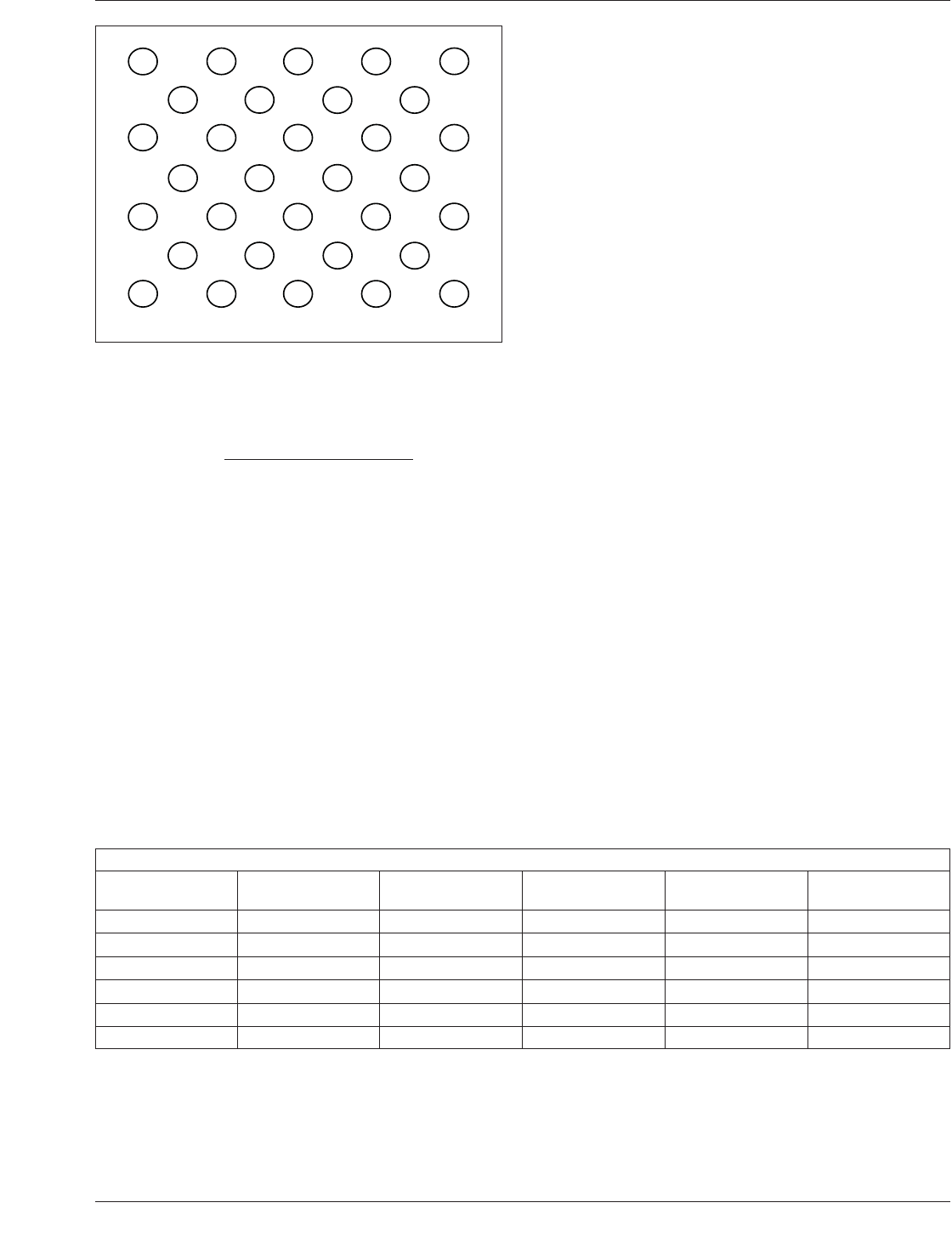
The following relationship can be used to determine the
number of conductors per outlet for an interspersed array.
C =
[(r−2)(c−2)+(r−1)(c−1)]−d
2(r+c−2)
If C turns out to be a fraction, then rounding it down will
give the lower number of conductors to be accommodated
between some adjacent balls, and rounding it up will pro-
vide the number of maximum conductors needed to be
accommodated between other adjacent balls. The fraction
gives the proportion of the two numbers.
The sizes of the solder land and via land also affect the
routing ability of BGA packages. A 0.8 mm solder land on
a 1.27 mm pitch leaves only 0.5 mm between solder lands
for routing. In order to get two conductors between the
solder lands, 100/100 µm conductors/spacing would need
to be used. However, if a 0.6 mm solder land is used, two
conductors can be routed between lands using 125/125 µm
conductors/spacing.
Because of the small space between solder lands on finer
pitch BGA (1.00 mm and less), smaller via lands and drill
sizes are required. As the drill sizes get smaller, the maxi-
mum allowable board thickness also decreases. This may
force board designers to use fewer layers or to decrease the
dielectric thickness between layers.
If microvias are used, this may force the outer two layers
of the PCB to be signal layers.
6.3.1 Escape Strategies Table 6-4 shows some escape
strategies for full arrays.
To accommodate a flip chip with area array I/O lands at
0.25 mm pitch, the BGA package substrate will need bond-
ing lands at 0.25 mm pitch on the top side, and solder balls
at 1.27 or 1.00 mm pitch on the bottom side. These oppos-
ing sets of lands must be connected by the BGA package
substrate (high-density microcircuit board) wiring and
interlevel vias or PTHs. It may be necessary to have one or
more interconnecting lines between two adjacent bonding
lands on the topside of the BGA substrate. This is done in
order to access multiple rows of the interior I/O lands for
connection to the vias or PTHs for eventual connection to
the solder balls on the bottom side. Very aggressive layout
rules must be used, even when designing with surface
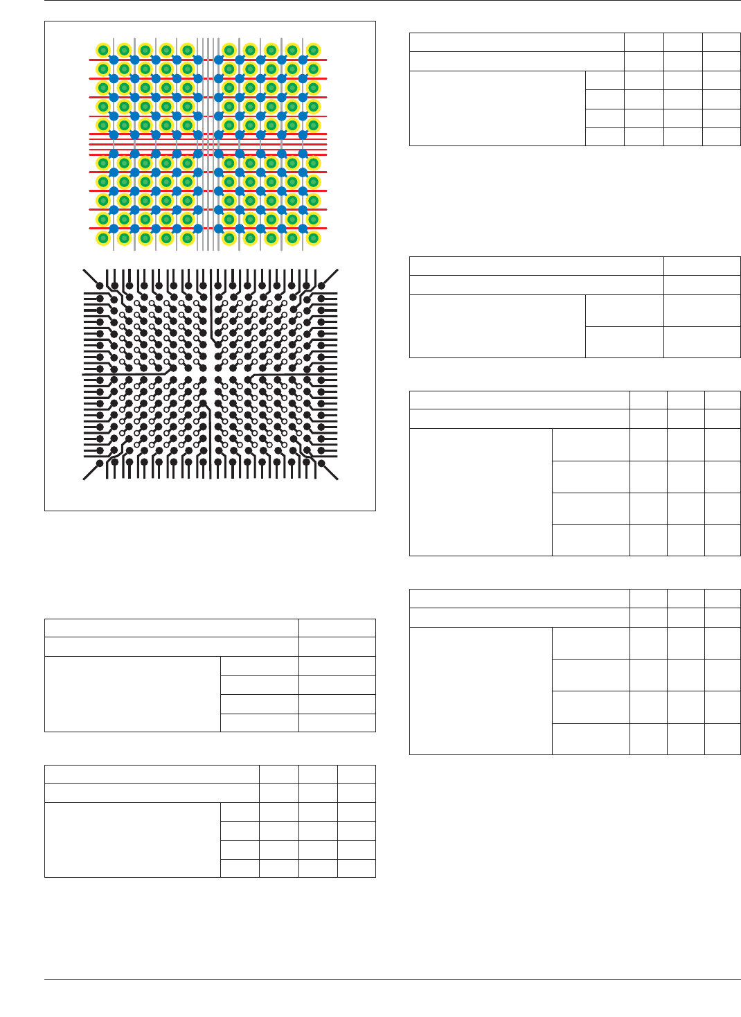
redistribution layers (see Figure 6-14).
For high performance chips with 1700 pin requirements,
a BGA with very dense wiring layers is required. The body
size of such a BGA would be 50 mm. In all probability,
there would be depopulated solder balls in the middle
of the BGA. Regarding pitch, such a BGA substrate
would require a 1.00 mm via and solder ball pitch, which
would accommodate a ball density of 100 I/O per square
centimeter.
IPC-7095c-6-13
Figure 6-13 Interspersed Array
Table 6-4 Escape Strategies for Full Arrays
Full array parts
Pitch (mm)
Nominal Ball
Diameter (mm) Surface Traces
Dog Bone
Through Vias
Dog Bone
Microvias Microvia in Pad
1.27 0.75 Y Y Y Y
1.0 0.45 - 0.6 Y Y Y Y
0.8 0.3 - 0.5 Y Y Y Y
0.75 0.3 - 0.45 N H, S Y Y
0.65 0.3 - 0.4 N N Y Y
0.5 0.3 N N N Y
Notes:
See Table 6-5 to 6-7 for details on routing channel widths
See Tables 6-8 to 6-10 via drill and land size assumptions used
Y = yes, with ‘‘standard’’ board fabrication capability and standard land size
H = high capability board fabrication required
S = shrink land size required
N = not practical with industry standard design & process
January 2013 IPC-7095C
57
Copyright IPC-Association Connecting Electronics Industries
Provided by IHS under license with IPC
Not for Resale
No reproduction or networking permitted without license from IHS
--`,,```,,,,````-`-`,,`,,`,`,,`---
6.3.2 Surface Conductor Details Tables 6-5 through 6-7
shows various conductor routing characteristics for differ-
ent BGA pitches.
6.3.3 Dog Bone Through Via Details Tables 6-8 through
6-10 provide the details for conductor routing using the
dogbone via concept. The tables also are organized per via
pitch.
6.3.4 Design for Mechanical Strain Mechanical strain
and board flexure are major causes of PCB and BGA joint
damage. Several BGA layout strategies have been devel-
oped that can help reduce the impact of mechanical strain
on the BGA.
IPC-7095c-6-14
Figure 6-14 Conductor Routing Strategy
Table 6-5 Conductor Routing - 1.27 mm Pitch
Nominal Ball Diameter (mm) 0.75
Typical Solder Land Diameter (mm) 0.55
Conductor Spacing Width (µm) 150 2
125 2
100 3
75 4
Table 6-6 Conductor Routing - 1.0 mm Pitch
Nominal Ball Diameter (mm) 0.6 0.5 0.45
Typical Solder Land Diameter (mm) 0.45 0.40 0.35
Conductor Spacing Width (µm) 150 1 1 1
125 1 1 2
100 2 2 2
75333
Table 6-7 Conductor Routing - 0.8 mm Pitch
Nominal Ball Diameter (mm) 0.45 0.4 0.3
Typical Solder Land Diameter (mm) 0.35 0.3 0.25
Conductor Spacing Width (µm) 150 1 1 1
125 1 1 1
100 1 2 2
75123
Table 6-8 Conductor Routing - 1.27 mm Pitch
Nominal Ball Diameter (mm) 0.75
Typical Solder Land Diameter (mm) 0.55
Drill Diameter 0.35 mm
[0.0135 in]
Y
0.3 mm
[0.012 in]
Y
Table 6-9 Conductor Routing - 1.0 mm Pitch
Nominal Ball Diameter (mm) 0.6 0.5 0.45
Typical Solder Land Diameter (mm) 0.45 0.40 0.35
Drill Diameter 0.35 mm
[0.0135 in]
NNY
0.3 mm
[0.012 in]
NYY
0.25 mm
[0.010 in]
YYY
0.2 mm
[0.008 in]
YYY
Table 6-10 Conductor Routing - 0.8 mm Pitch
Nominal Ball Diameter (mm) 0.45 0.4 0.3
Typical Solder Land Diameter (mm) 0.35 0.3 0.25
Drill Diameter 0.35 mm
[0.0135 in]
NNN
0.3 mm
[0.012 in]
NNN
0.25 mm
[0.010 in]
NYY
0.2 mm
[0.008 in]
YYY
IPC-7095C January 2013
58
Copyright IPC-Association Connecting Electronics Industries
Provided by IHS under license with IPC
Not for Resale
No reproduction or networking permitted without license from IHS
--`,,```,,,,````-`-`,,`,,`,`,,`---
PCB:
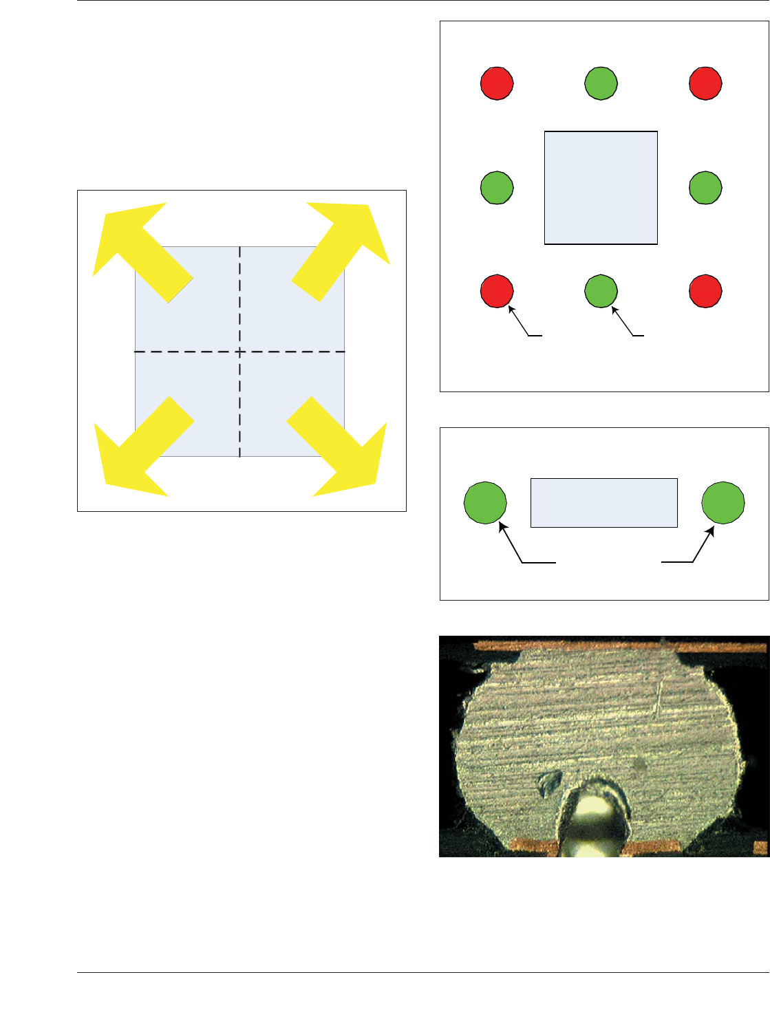
• Divide each BGA into four equal quadrants with lines
parallel to the sides. From each quadrant, route conduc-
tors and dogbones to escape vias from the BGA lands so
that they go out radially from the BGA at 45 degree
angles (see Figure 6-15). This increases the amount of
strain that corner lands can withstand before damage.
• Enlarge or teardrop the dogbones or routes to BGA cor-
ner lands.
PCA and Enclosures:
• Do not place screws near BGA corners in line with the
package diagonals (see Figure 6-16, red locations).
• Preferably place screws and bosses on the normal to the
midpoint of the BGA sides (see Figure 6-16, green loca-
tions).
• Use header connectors with a stiff body and provide PCA
support at both ends, especially for connectors with high
insertion and release forces (see Figure 6-17).
• Use washers under screw heads not larger than the boss
Outer Diameter to minimize torsional deformation of the
PCB.
6.3.5 Uncapped Via-in-Pad and Impact on Reliability
Issues
Via-in-pad (through-hole via, capped on bottom of
the board) for BGA lands can cause voids in the BGA
solder joints, which may impact reliability. Current data
indicate that, for the standard 25-35 mm package with
0.75 mm balls, there is no reliability risk from voids.
Accelerated aging tests have been performed and the fail-
ure rate was statistically equivalent to standard dogbone
designs. An illustration of the problem is shown in Figures
6-18 and 6-19.
IPC-7095c-6-15
Figure 6-15 BGA Dogbone Land Pattern Preferred Direc-
tion for Conductor Routing
Dogbone
Direction
Dogbone
Direction
Dogbone
Direction
Dogbone
Direction
BGA
IPC-7095c-6-16
Figure 6-16 Preferred Screw and Support Placement
BGA
AVOID
CORNER
PLACEMENT
PREFERRED
PLACEMENT
SCREW AND SUPPORT PLACEMENT
IPC-7095c-6-17
Figure 6-17 Connector Screw Support Placement
CONNECTOR SCREW SUPPORT
PROVIDE END
CONNECTOR
SUPPORT ON PCB
Figure 6-18 Cross Section of 0.75 mm Ball with Via-in-
Pad Structure (Indent to the Upper Left of the Ball is an
Artifact.)
January 2013 IPC-7095C
59
Copyright IPC-Association Connecting Electronics Industries
Provided by IHS under license with IPC
Not for Resale
No reproduction or networking permitted without license from IHS
--`,,```,,,,````-`-`,,`,,`,`,,`---