IPC-7095C-2013.pdf - 第21页
Placing signal pin assignments on the outer rows of an array package, and using the inner balls for power and ground will facilitate escape routing. However , the corner balls of large array packages are more susceptible…
The signal I/O escape wiring, and their interconnection to
other high I/O packages, will also require High Density
Interconnect (HDI) technology. As the number of I/O on a
chip increases further, the body size of the single chip
package may become unacceptably large and could require
reassessment of the overall package solution, including
considering multichip module packaging or Application
Specific Module Packaging (ASMP) as an alternative. The
signal I/O count for high performance BGAs is about 2.5X
that commonly required for BGAs used in handheld prod-
ucts. The interconnection density requirement is linearly
proportional to the number of signal I/O per package, and
inversely proportional to the center-to-center pitch between
adjacent packages. A 2.5X increase in signal I/O from 500
to 1300 pins per package at the same package-to-package
pitch will require a printed board with a 2.5X increase in
its wiring density, and a proportional increase in the den-
sity of the inter-level vias or Plated-Through Holes (PTHs).
This may require a reduction in the PTH/via pitch, and an
increase in the number of signal layers in the printed board.
With more of the circuit customization going into silicon
and with the component package size increasing, the
printed board design will need to change. The higher I/O
demand will require multilayer or high density interconnec-
tion (microvia) designs to support the required wiring and
to provide escape routing from the internal connections of
array component patterns to the printed board. Both sides
of the printed board may be required to place all the com-
ponents required by the design. There will also be an
increased demand on the printed board to handle the
required power dissipation.
Using high I/O components like BGAs and fine pitch
BGAs creates the challenge of routing all the required sig-
nal, power, and ground I/O balls to the printed board with-
out increasing board complexity and, therefore, cost.
Thoughtful package pin assignments and the package
configuration considerations (pitch, ball size, ball count,
and depopulation) can go a long way in making the board
routing easier.
Two interconnection signal layers can be sufficient for
BGA package escape, even when the BGA has very high
ball counts, provided that the pin assignments are properly
planned and the escape routing is carefully designed. Table
3-2 indicates the number of ‘‘escapes’’ possible on two
layers of circuitry vs. the array size and the number of
conductors between lands/vias. It should be noted that, as
the number of I/O increases, the ability to escape dimin-
ishes, and thus more layers may be required. At first
glance, Table 3-2 might appear to indicate that two routing
layers are insufficient to escape any array greater than 16 x
16 (256 balls). In reality, a significant number of the balls
will be used for power and ground connections and there-
fore do not need ‘‘escape’’ routing. They can be directly
connected to the appropriate plane through the dogbone via
attached to the land. That being said, poor placement of the
signal or power/ground balls can ‘‘waste’’ available routing
channels and significantly reduce the total number of sig-
nal I/Os that can be routed out in a given number of layers.
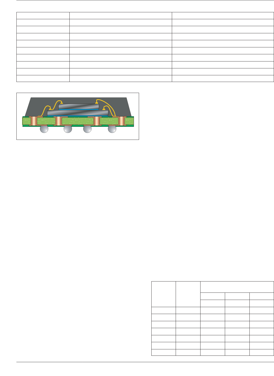
Table 3-1 Multichip Module Definitions
MCM Technology Description Attributes
Type 1 Common Technology Package Multiple same type chips, in plane.
Type 1S Common Technology Package Multiple same type chips, stacked.
Type 1F Common Technology Package Multiple same type chips, folded.
Type 2 Mixed Technology Package Mixed IC technology package, in plane.
Type 2S Mixed Technology Package Mixed IC technology package, stacked.
Type 2F Mixed Technology Package Mixed IC technology package, folded.
Type 3 System in Package Mixed ICs and discrete devices, in plane.
Type 3S System in Package Mixed ICs and discrete devices, stacked.
Type 4 Optoelectronic System Package Mixed technology for optoelectronics.
IPC-7095c-3-4
Figure 3-4 MCM Type 2S-L-WB
Table 3-2 Number of Escapes vs.
Array Size on Two Layers of Circuitry
Array Size
Total
Leads
Number of Conductors
Between Vias (•|•)
123
•|• •||• •|||•
14 X 14 196 192 196 196
16 X 16 256 236 256 256
19 X 19 361 272 316 352
21 X 21 441 304 356 400
25 X 25 625 368 436 496
31 X 31 961 464 556 640
35 X 35 1225 528 638 736
IPC-7095C January 2013
6
Copyright IPC-Association Connecting Electronics Industries
Provided by IHS under license with IPC
Not for Resale
No reproduction or networking permitted without license from IHS
--`,,```,,,,````-`-`,,`,,`,`,,`---
Placing signal pin assignments on the outer rows of an
array package, and using the inner balls for power and
ground will facilitate escape routing. However, the corner
balls of large array packages are more susceptible to
mechanical failure and, therefore, it may be better to use
these for redundant ground connections. The number of
rows of signal I/O that can be routed out will depend on the
desired number of conductor routing layers in the printed
board and the number of conductors that can be routed
between lands and vias.
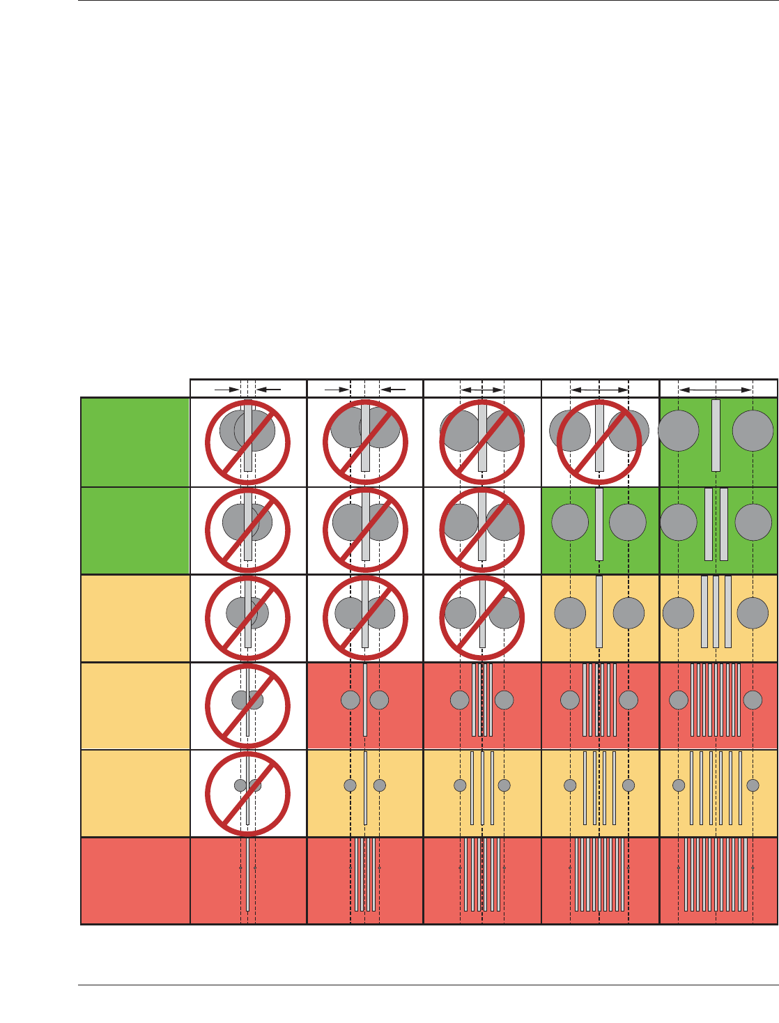
Figure 3-5 shows examples of conductor and space widths
that will fit between adjacent lands with various pitches
and land diameters. Note that as the ball pitch decreases,
the conductor width and spacing for a given number of
conductors per channel also decreases, and it becomes
more difficult and costly to produce the board.
Using 150 µm conductors and spaces is quite cost effective,
but printed board cost begins to increase significantly for
100 µm conductors and spaces. Using an organic intercon-
necting substrate to mount the bare die within a plastic
BGA requires that the mounting lands on the substrate
match the bonding lands on the die.
The bonding lands are typically positioned for wire bond-
ing, since this is the most popular technique. Thermally
conductive adhesive is one of the methods used to attach
the back of the die to the substrate. Depending on the
number of I/O and the lead pitch, multilayer substrate fab-
rication techniques may be used to translate a peripheral
bonding land die, to an area array matrix of bumps, balls,
or columns (see Figure 3-6).
The transition of chip bonding lands that are in an array
format permits the mounting of the die in flip chip configu-
rations. In this instance, the die is mounted opposite to that
which is wire-bonded and the bumps of the die come into
direct contact with the substrate being used to convert the
die pattern to the BGA pattern. This creates new challenges
Figure 3-5 Conductor Width to Pitch Relationship
Conventional FR-4
125 µm Line
125 µm Space
700 µm Land
Conventional FR-4
125 µm Line
125 µm Space
600 µm Land
High Density FR-4
100 µm Line
100 µm Space
600 µm Land
Next Gen FR-4
60 µm Line
50 µm Space
300 µm Land
Next Gen Microvia
50 µm Line
50 µm Space
50 µm Land
Typical Microvia
75 µm Line
100 µm Space
200 µm Land
0.25 mm Pitch 0.5 mm Pitch 0.75 mm Pitch 1.0 mm Pitch 1.27 mm Pitch
January 2013 IPC-7095C
7
Copyright IPC-Association Connecting Electronics Industries
Provided by IHS under license with IPC
Not for Resale
No reproduction or networking permitted without license from IHS
--`,,```,,,,````-`-`,,`,,`,`,,`---
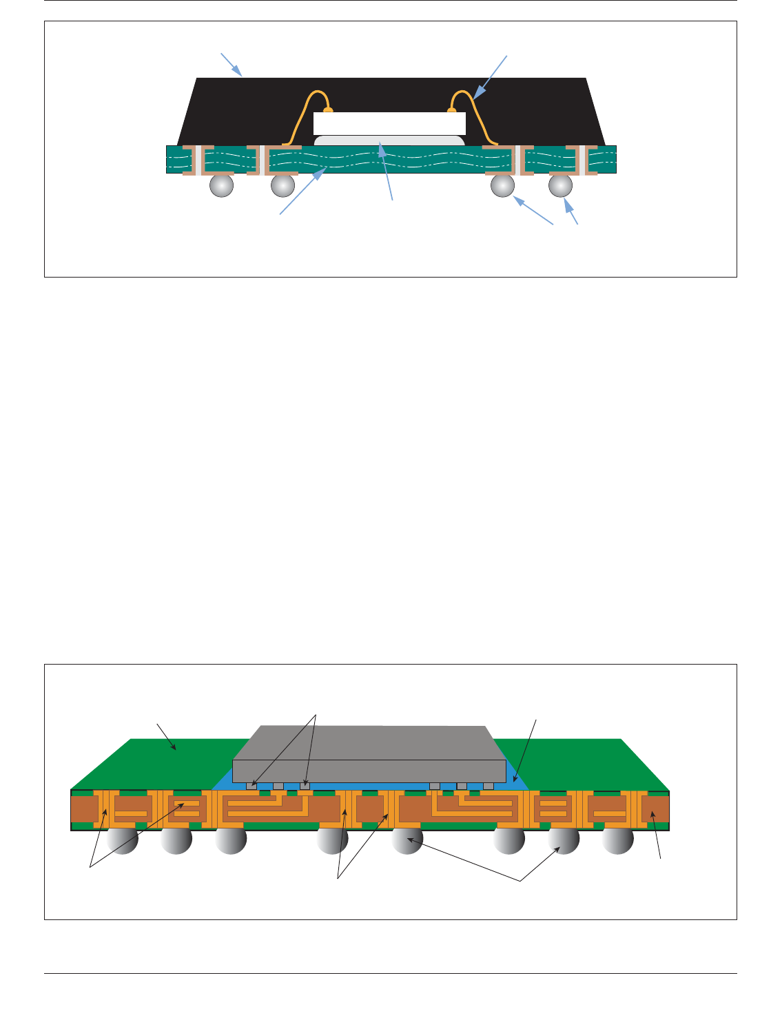
for the routing requirements for the organic high-density
microcircuit board manufacturer. In addition, underfill is
usually required to accommodate and soften the mismatch
between the coefficient of thermal expansion (CTE) of the
chip and the CTE of the organic multilayer board (see
Figure 3-7).
3.1.3 Assembly Equipment Impact Implementing BGA
technology may require some new assembly capability.
Depending upon the type of pick and place systems, a
change in package carrier mechanism may also be required
to transfer packages from matrix tray to the pick position.
Fiducials may also help vision systems recognize the exact
location of the land pattern for the BGA, similar to what is
used for fine-pitch peripheral leaded parts. Large BGA
parts on tape-and-reel will require 44 mm and 56 mm feed-
ers depending on the body size. Use of a forced air convec-
tion oven is preferred. Repair and inspection of BGAs are
rather difficult. Rework machines with paste deposition,
preheat, and vision capability may not be required, but are
very helpful. X-ray and optical inspection (endoscope)
capability for process development is a benefit.
3.1.4 Stencil Requirements The stencil thickness may
need to be reduced when using finer pitch BGA parts. Sten-
cil thickness and land size will determine paste volume,
which is very critical for ceramic BGAs. It is helpful to
have trapezoidal stencil apertures (slightly larger opening
on the bottom than on the top) for better paste release.
Generally, on larger BGA components with 1.25 mm and
1.00 mm pitch, the aperture is large enough that stencil
clogging, print registration and definition are less of a prob-
lem than with quad flat pack (QFP) components.
Matching solder paste stencil openings to the requirements
of fine-pitch BGAs requires an understanding of the rela-
tionship between the stencil aperture and the size of the
particles in the paste. IPC-7525 provides good descriptions
to help make the appropriate relationship decisions as the
land patterns for attachment become smaller and are closer
to one another.
Overmolded Epoxy
BT Substrate
Wire Bonds
Die Attach
Solder Balls
(Sn63Pb37)
Silicon Die
IPC-7095c-3-6
Figure 3-6 Plastic Ball Grid Array, Chip Wire Bonded
IPC-7095c-3-7
Figure 3-7 Ball Grid Array, Flip Chip Bonded
High Melt Temperature Solder
or Z-Axis Interconnection Material
Soldermask
Epoxy Underfill
Copper Circuitry
and Plated Vias
Thermal Vias
Solder Balls
IC chip
High Performance
Laminate Material
IPC-7095C January 2013
8
Copyright IPC-Association Connecting Electronics Industries
Provided by IHS under license with IPC
Not for Resale
No reproduction or networking permitted without license from IHS
--`,,```,,,,````-`-`,,`,,`,`,,`---