IPC-7095C-2013.pdf - 第158页
9.4.3 Evidence of Dewetting 9.4.4 Mottled Condition 9.4.5 Tin/Lead Solder Ball Evaluation 9.4.6 SAC Alloy Possible Cause Dewetting of the solder at the contact interface may be due to excessive oxidation on the land, org…
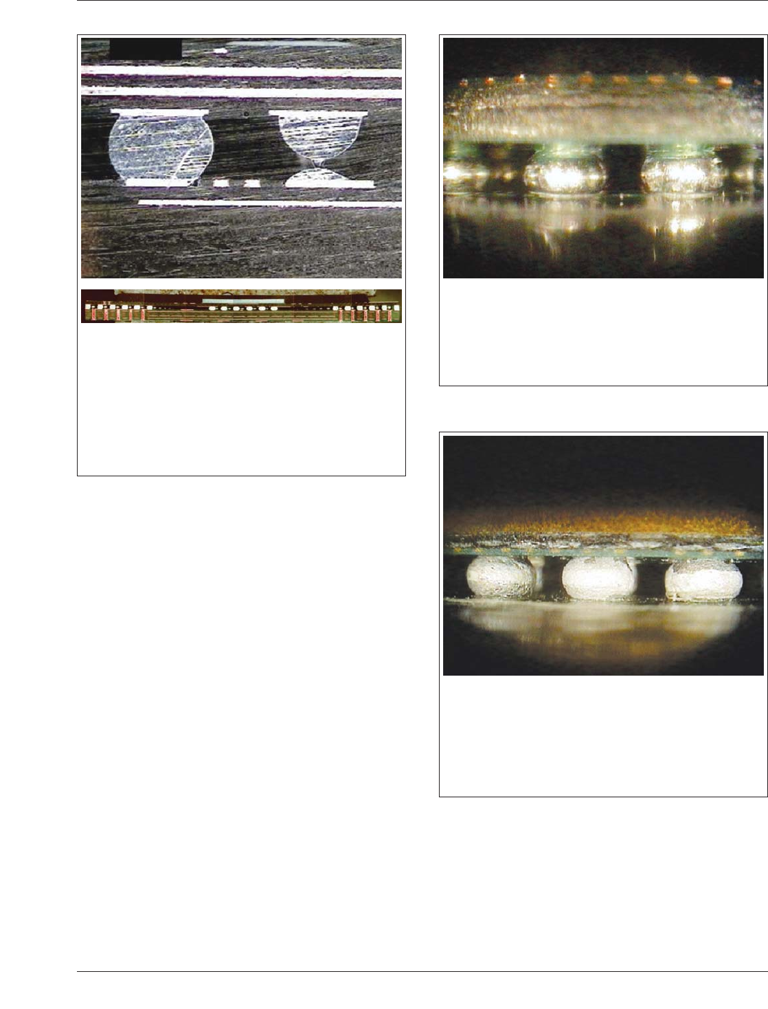
9.3.2 Solder Joint Opens Due to Interposer Warp
9.4 Solder Joint Conditions
The following sections deal
with the conditions of the solder ball in relationship to the
mounting structure and the component interposer. In each
instance, an explanation is provided as to the reason for the
occurrence of the condition.
9.4.1 Target Solder Condition
9.4.2 Solder Balls with Excessive Oxide
Possible Cause
– The failure appears to be due to insufficient paste release
from the stencil or insufficient ball size.
– Warped package (smiling BGA) with corner balls lifted up.
Potential Solution
– Check balls at incoming prior to assembly.
– Return package to supplier.
– Implement incoming inspection and/or source audit.
– Apply extra solder paste on corner lands.
Possible Cause
Solder balls exhibit a uniform shape and texture, and they are
symmetrically aligned to the attachment sites, showing ball col-
lapse on both top and bottom of BGA balls.
Potential Solution
Document process parameters and maintain a stable process.
Possible Cause
Solder ball oxides will form due to exposure to multiple reflow
solder cycles (topside or bottom side).
Potential Solution
This can be reduced significantly by correct flux selection,
reducing the number of production reflows to two and not
cleaning the PWB between reflows.
January 2013 IPC-7095C
143
Copyright IPC-Association Connecting Electronics Industries
Provided by IHS under license with IPC
Not for Resale
No reproduction or networking permitted without license from IHS
--`,,```,,,,````-`-`,,`,,`,`,,`---
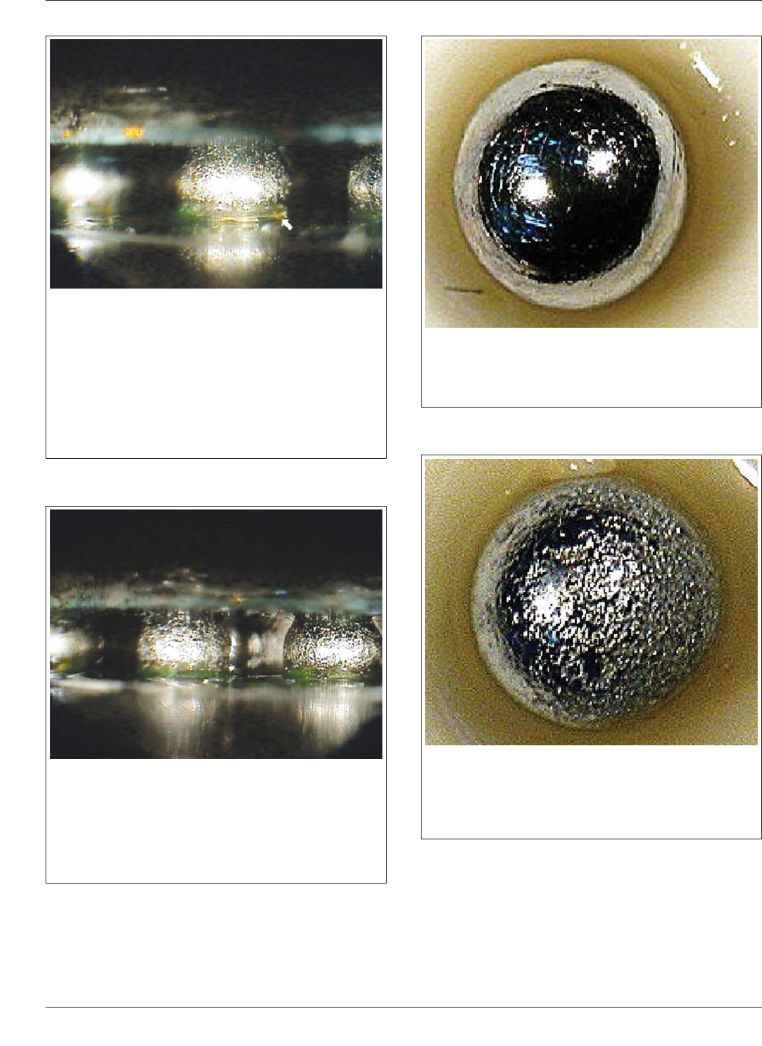
9.4.3 Evidence of Dewetting
9.4.4 Mottled Condition
9.4.5 Tin/Lead Solder Ball Evaluation
9.4.6 SAC Alloy
Possible Cause
Dewetting of the solder at the contact interface may be due to
excessive oxidation on the land, organic contamination. Poor
plating can contribute to this condition as well. ENIG comes in
a number of systems, i.e., hi P and low P systems. Dewetting
of ENIG is due to oxidation of Ni barrier not excess P on sur-
face.
Potential Solution
Develop process effect controlled experiment to determine
which attribute contributes most to dewetting.
Possible Cause
The surface condition of the solder ball is likely the result of
overheating during the reflow solder process or excessive/
repeated exposure to temperatures above liquidus.
Potential Solution
Evaluate reflow process in order to determine proper ball char-
acteristics.
Possible Cause
Reflow of solder paste should form a proper ball geometry.
Potential Solution
Maintain process effects standardization.
Possible Cause
Slightly mottled appearance of the tin-silver-copper alloy.
Potential Solution
Determine paste and ball characteristics through experimenta-
tion.
IPC-7095C January 2013
144
Copyright IPC-Association Connecting Electronics Industries
Provided by IHS under license with IPC
Not for Resale
No reproduction or networking permitted without license from IHS
--`,,```,,,,````-`-`,,`,,`,`,,`---
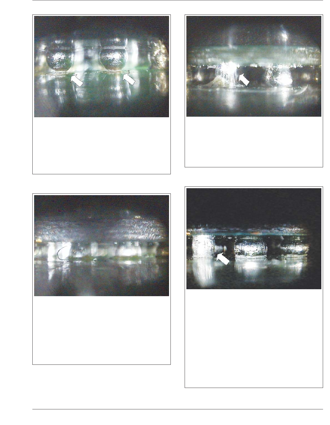
9.4.7 Cold Solder Joint
9.4.8 Incomplete Joining Due to Land Contamination
9.4.9 Deformed Solder Ball Contamination
9.4.10 Deformed Solder Ball
Possible Cause
The ball contacts have not completed wetting at the attach-
ment sites. Condition may be due to poor solder paste printing
or contamination on the attachment site that cannot accept
wetting.
Potential Solution
Check stencil and printing process to determine sufficient sol-
der paste deposit.
Possible Cause
Organic contamination or oxidation of the PCB land can nega-
tively compromise the uniform and complete joining of the sol-
der ball and PCB land surface. PCB land was not sufficiently
clean to promote proper wetting prior to application of solder
paste.
Potential Solution
Test for cleanliness as part of process. Implement proper PCB
storage and handling procedures to prevent contamination and
exposure to conditions which promote oxidation.
Possible Cause
Solder ball deformation can occur due to the component mov-
ing during the reflow soldering process (package warp or board
warp) and/or when the land pattern geometry is not correct.
Potential Solution
Avoid overheating which causes quality disparities of the inter-
poser.
Possible Cause
Ball deformation (column shaped) can result from temporary
warping of the substrate during reflow soldering. The package
substrate corner, in this case, moved upward at the higher
temperature, away from the board surface. While in this condi-
tion, the solder alloy cooled to a solidus condition resulting in a
column shape. This is known as dynamic warping because the
warping increases along with the reflow temperature. As it
cools, the package would return to its original shape if the
solidified solder was not preventing it from doing so.
Potential Solution
This is caused by CTE mismatch of the materials in the pack-
age or board. Though elimination of this condition is outside the
control of the SMT process, the effect can be minimized by
avoiding overheating of the interposer and the board.
January 2013 IPC-7095C
145
Copyright IPC-Association Connecting Electronics Industries
Provided by IHS under license with IPC
Not for Resale
No reproduction or networking permitted without license from IHS
--`,,```,,,,````-`-`,,`,,`,`,,`---