IPC-7095C-2013.pdf - 第146页
may make it necessary to place large BGAs at the edges of the board. In such cases, the reflow soldering process win- dow will be narrowed to keep the maximum temperature the BGA components are exposed to below acceptable…

• Mechanical, electrical and thermal properties
• Reworkability
• Compatibility with lead (during transition period)
• Availability from suppliers
• Cost
• Patent concerns
Table 8-4 compares the composition selected by three con-
sortia. The compositions are very close to each other and
behave very similarly in the reflow soldering process. Fur-
ther, solder alloy suppliers usually state a tolerance of ±
0.2% by weight for each elemental component of the sol-
der, which is consistent with the ANSI J-STD-006 specifi-
cation. When taking this into consideration, the alloy com-
positions below all overlap.
8.5.5.2 Recommendations for Alloys with Ag Content
Around 1%
• Solder joints must reach a minimum of 235°C with a TAL
of at least 60 seconds.
• Reflow profiles for some PCAs may need to be modified
when BGAs with low Ag alloys are used
• At a minimum, reflow profiles may need to be validated
using metallography, requiring additional engineering
effort
Along with careful oven profiling, metallography should be
performed (with statistically significant sample sizes) to
validate that components with low Ag solder ball alloys are
forming proper joints.
The number of thermocouples used to validate a profile
should be significantly increased so that the low-Ag com-
ponent can be shown to meet the conditions given above,
and that all other components meet the existing specifica-
tions (no overheating).
The 1% Ag alloys appear to be incompatible with many
current industry lead-free assembly specifications for
SAC305 that require a minimum reflow peak temperature/
TAL of 235°C/60 sec, while current specifications are
likely adequate for other alloys. The actual limit in Ag
content at which significant change to the lower limit of the
reflow profile is needed has not been precisely identified. It
appears to be between 1% and 2.3% Ag. Other variables
may impact this value, so caution is warranted for any
alloy with less than 3% Ag.
Reliability of Solder Joints – Industry studies consistently
indicate better drop performance for low Ag alloys than for
near-eutectic SAC. Results depend on the solder land fin-
ishes in addition to alloy composition. The exact reason for
the improvement is still being debated. It may be due to
reductions in the stiffness and yield strength of the bulk
solder ball. It is known that changes to the intermetallic
layer composition and/or structure of the solder joint can
be expected. A reduction in under cooling is required to
solidify the BGA ball.
The published data indicates that the fatigue life of low Ag
alloys is lower than the higher Ag counterparts. However,
the existing models are very product-specific. There are
currently no agreed-to acceleration models available for
these alloys, making product life predictions difficult. The
existing study results available relate to various end-
product conditions, thus understanding how those low Ag
alloys perform relative to eutectic tin/lead is not easy.
Managing the Change to a Low Ag Ball Alloy – Due to
the potential impacts on reflow process window and reli-
ability, changing from a near-eutectic SAC ball alloy to one
with less than 3% Ag should be considered to be a change
in form, fit, or function. In this case a change in part num-
ber for any BGA component, where the only change is ball
alloy, is considered appropriate.
8.5.5.3 Board Design Considerations Board Design for
BGA Assembly with Lead-Free Solders is generally very
similar to that for presently used tin/lead solders. The same
Design for Manufacturability (DfM) rules and guidelines
should be applied for lead-free boards as those used to tin/
lead (SnPb) boards. These include consideration for com-
ponent orientation, soldering, via holes, solder mask,
repairability and testability. Some of these are described
further below.
BGA Land Pattern Designs – As in the case of tin/lead
BGA soldering, the preferred BGA Land style for SnAgCu
soldering is the nonsoldermask-defined design as opposed
to the soldermask-defined land style since it allows the
maximum flexibility for the PCB designer, and less stress
points are introduced to the solder joint by the solder mask.
Component Placement Location on the PCB – Since
SnAgCu solders require higher reflow temperatures for
component soldering, the placement location of large, tem-
perature sensitive BGA components may need to be
addressed carefully. The regions near the edges of the
board are, depending on the board size, thickness and layer
count, typically 5-15°C higher in temperature than those in
the central locations. Since large packages are more prone
to moisture and thermal stress induced defects when sub-
jected to higher reflow temperatures, such packages, if pos-
sible, should be confined to the central regions of the
board. Other factors, such as trace routability and density,
Table 8-4 Comparison of Lead-Free
Solder Alloy Compositions in The Sn-Ag-Cu
Family Selection by Various Consortia
Consortium % Sn % Ag % Cu
IDEAL 95.5 3.8 0.7
Solder Products Value Council 96.5 3.0 0.5
iNEMI 95.5 3.9 0.6
January 2013 IPC-7095C
131
Copyright IPC-Association Connecting Electronics Industries
Provided by IHS under license with IPC
Not for Resale
No reproduction or networking permitted without license from IHS
--`,,```,,,,````-`-`,,`,,`,`,,`---
may make it necessary to place large BGAs at the edges of
the board. In such cases, the reflow soldering process win-
dow will be narrowed to keep the maximum temperature
the BGA components are exposed to below acceptable lim-
its.
8.5.5.4 Reflow Soldering Considerations Reflow sol-
dering is commonly done in an IR convection oven with
heated air convection. Despite the higher reflow tempera-
tures necessary to melt the SnAgCu (SAC) solders when
compared with the tin/lead solders, new equipment may
not be necessary for lead-free reflow soldering. The same
ovens as used before for tin/lead solders can be used with
the obvious increase in the settings for the various heating
zones in the reflow oven. As the PWB mass increases the
ability to limit the maximum reflow temperature, delta T
across the PWB and reflow time becomes more difficult
without extended zone ovens.
The environment in the oven can be either air or inert, such
as nitrogen. For lead-free soldering, to minimize the oxida-
tion of the materials on the board assemblies during the
high temperature reflow operation, an inert atmosphere can
be helpful. A lot of the criteria depends on the solder paste
and the solder paste manufacturer as well as the thermal
mask of the electronic assembly. Some board surface fin-
ishes, such as organic solderability preservatives (OSP) on
copper may require an inert atmosphere during reflow sol-
dering to attain acceptable solder joint yield levels.
A reflow solder profile should be developed for all board
assemblies. Since SAC solders require higher reflow sol-
dering temperatures, it is important to determine the maxi-
mum temperature at various different locations on the
board. Component temperatures may vary because of mate-
rial type, surrounding components, location of part on the
board, and package densities.
To avoid moisture and thermo-mechanical stress induced
failures on plastic components, it is best to measure the
temperature of the component body and check to ensure
that it doesn’t exceed the maximum temperature it is rated
for. Hence, thermocouples, which are generally used to
measure the temperatures during reflow profiling, should
be attached at the solder joint as well as the body of the
various components during reflow profiling of board
assemblies. Large components generally have greater than
5°C difference between the leads/solder balls and the mold-
ing compounds of the component.
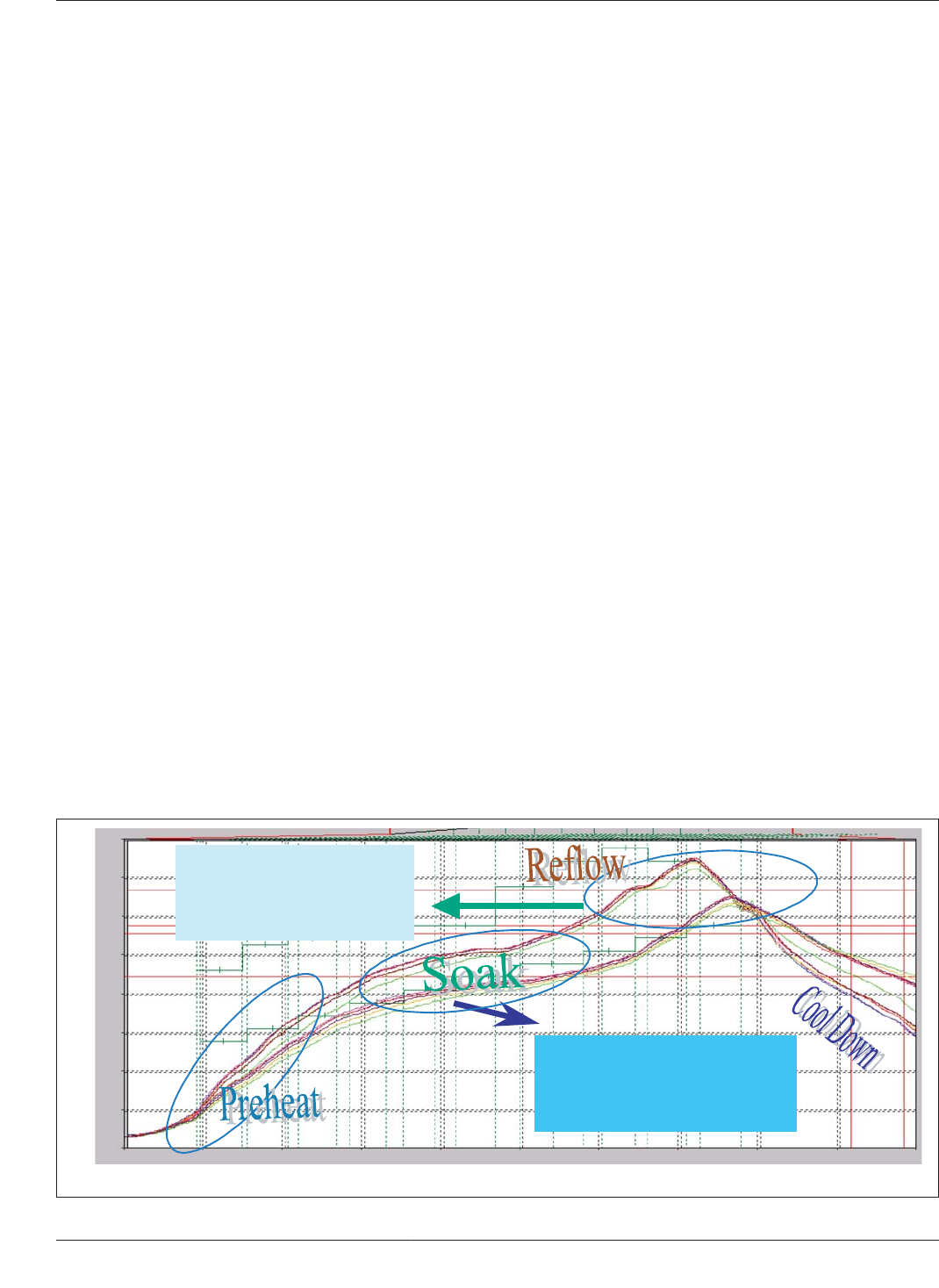
A typical SAC reflow profile is compared with a tin/lead
reflow profile for a BGA solder joint in Figure 8-21 below.
Four different regions of the reflow profile are shown: the
Preheat region during which the low melting volatile ingre-
dient in the solder paste vehicle are evolved; the Flux Acti-
vation region which enables the temperature to start equili-
brating across the board and to start to activate the flux; the
Reflow region where the solder melts, wets the land surface
and forms the solder joint; and finally the Cool down stage,
where the solder solidifies and the board assembly exits the
oven to be cooled down by forced air blown down on the
board by fans.
The profiles illustrated in Figure 8-21 are termed ‘‘FAT’’
(flux activation time) profiles since they have a soak zone
before the solder is reflowed. Alternatively, ‘‘ramp’’ pro-
files can also be developed which contain a continuous
ramp from the preheat zone to the reflow soldering zone.
These ramp profiles increase the throughput of the board
assemblies in the reflow ovens. But, care should be taken
to avoid overheating of components, particularly on the
edges of the boards.
8.5.5.5 Appearance of BGA Lead-Free Solder Joints The
BGA package body obscures its solder joints. However,
IPC-7095c-8-21
Figure 8-21 Comparison of a Lead-Free (SnAgCu) and Tin/Lead (SnPb) BGA Reflow Soldering Profiles
Tin-Lead Solder Profile
Reflow @ 183°C
Peak Temp. = 205 to 220°C
Lead Free Solder Profile
Reflow @ 217°C
Peak Temp = 235 to 245°C
257
227
197
167
137
107
77
47
17
0.0
0.6
1.2
1.8 2.4 3.0 3.6 4.2 4.8
5.4
6.0
Temperature
Time in Minutes
IPC-7095C January 2013
132
Copyright IPC-Association Connecting Electronics Industries
Provided by IHS under license with IPC
Not for Resale
No reproduction or networking permitted without license from IHS
--`,,```,,,,````-`-`,,`,,`,`,,`---
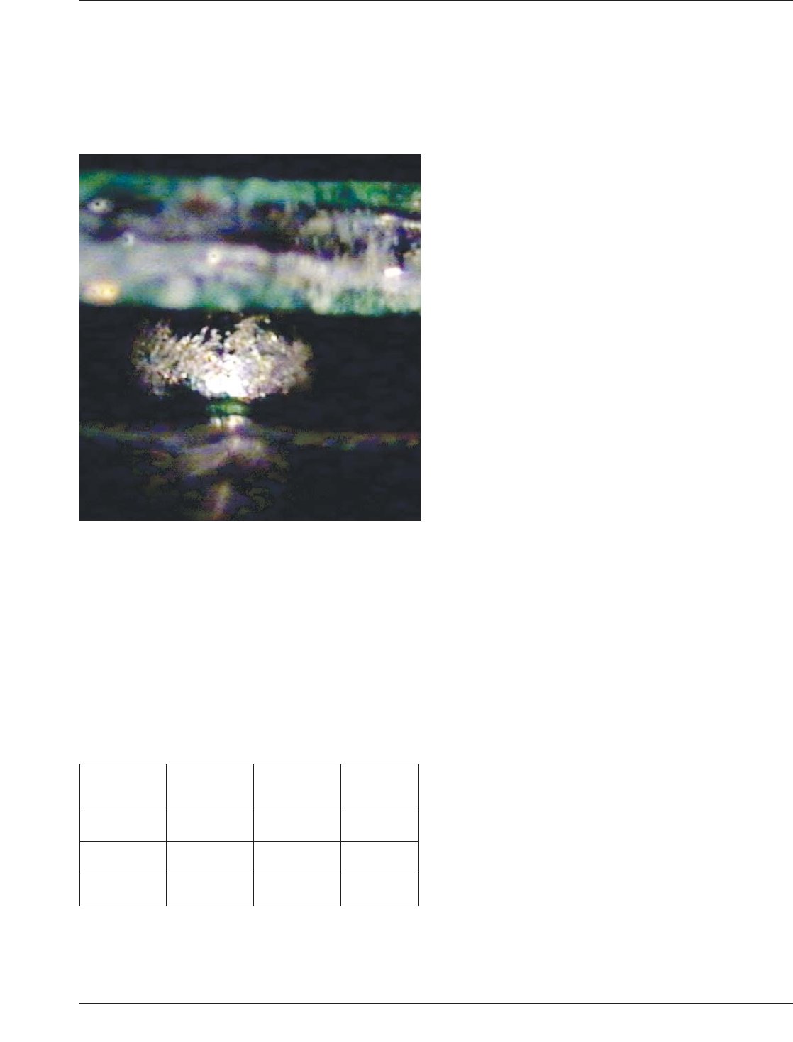
with the help of special microscopes such as the endo-
scope, peripheral solder joints can be viewed. SnAgCu sol-
der joint microstructures are multiphase microstructures
and the surface of the solder joints appears rough. Figure
8-22 shows a typical SnAgCu BGA solder joint. This is
much different from typical SnPb BGA solder joints which
usually have a shiny surface. Ball
8.5.5.6 Transition Lead-Free Technologies The transi-
tion from a total tin/lead soldering system to a total lead-
free soldering system is not going to happen overnight.
There may be an interim phase where tin/lead and lead-free
solders will co-exist on board assemblies. This transition
phase entails that the impact of lead in the SAC solder be
evaluated for impact on solder joint yields and reliability.
The likely lead-free board assemblies during this transition
phase are listed in Table 8-5.
The first possible lead-free board assembly listed above is
‘‘forward compatibility.’’ The board assembly soldering
process for forward compatibility assemblies has been con-
verted to lead-free technology with a change in the solder
paste composition and the reflow soldering profile to match
this change. However, some components, such as BGAs
that are soldered on the board, will still have tin/lead sol-
der due to the component supplier’s lead-free roadmap
having a conversion date later than the board assembler’s
conversion date. This results in the tin/lead solder joints of
the BGA-type components being ‘‘contaminated’’ by the
lead replacement metals in the lead-free solder paste.
The second possible lead-free board assembly listed above
is ‘‘backward compatibility.’’ Backward compatibility sce-
narios arise when component suppliers introduce the lead-
free components, but not all board assemblers that use
these components have converted their board assembly
lines to lead-free technology. These assemblers will still be
soldering the lead-free components with eutectic tin/lead
solder paste using tin/lead reflow soldering profiles. A tin/
lead component would obviously be preferable in this case,
but the component suppliers may, due to economic reasons,
not want to carry two component line items, one tin/lead
and one lead free, for the same device. The solder joints
formed with this combination of tin/lead solder paste and
lead-free solder ball will have a mixed composition. When
soldering a Ball Grid Array package with SnAgCu lead-
free solder balls using tin/lead solder paste, two different
scenarios arise based on the reflow profile used. The two
reflow profiles compared are shown in Figure 8-23 with the
total lead-free reflow profile also shown for comparison.
The tin/lead reflow profile, which is illustrative of the pro-
file used today for tin/lead assemblies, does not exceed the
melting point of the BGA’s SnAgCu solder ball. When a
reflow profile is unable to make lead-free solder ball melt
or dissolve, the solder joint yield and/or solder joint fatigue
life may suffer. The tin/lead solder paste deposited on the
lands of the solder balls melts but the SnAgCu solder balls
are still not molten. In such a material combination, the
lead may likely diffuse through the grain boundaries of the
solder ball. How high the lead from the tin/lead solder dif-
fuses up the SnAgCu solder ball will depend on how high
the reflow temperature gets and for how long the tin/lead
solder is molten. As shown in Figure 8-24, which depicts a
micrograph of a cross-section of a SnAgCu solder ball of a
BGA package soldered to a board using a reflow profile
which is unable to melt or dissolve SnAgCu solder ball, the
resulting solder joint microstructure is inhomogeneous.
This deleteriously impacts the solder joint reliability.
Yield impact on such solder joint is also deleterious due to
two reasons. One is due to the poor self-alignment of the
BGA during reflow soldering because the solder ball does
not become molten. This creates a potential for open joints
when the component is misaligned to some extent during
or after the Placement process step. Secondly, the lack of
‘‘ball collapse’’ may cause open solder joints from a lack of
contact between the solder paste deposit and the solder
ball.
Figure 8-22 Endoscope Photo of a SnAgCu BGA Solder
Ball
Table 8-5 Types of Lead-Free Assemblies Possible
Definition
Component
Termination/
BGA Ball Solder Paste
Board
Surface
Finish
Forward
compatibility
contains lead lead-free
leaded or
lead-free
Backward
compatibility
lead-free 63Sn37Pb
leaded or
lead-free
Total
lead-free
lead-free lead-free lead-free
January 2013 IPC-7095C
133
Copyright IPC-Association Connecting Electronics Industries
Provided by IHS under license with IPC
Not for Resale
No reproduction or networking permitted without license from IHS
--`,,```,,,,````-`-`,,`,,`,`,,`---