IPC-7095C-2013.pdf - 第94页
Reflowing OSP in nitrogen may also preserve the wettabil- ity of the lands for downstream processes as well as mini- mize oxidation of the test points or vias which may have an impact at in-circuit test (ICT). 7.1.4.3 Tim…
nozzle must gasket against the part, not allowing vacuum
leakage. Tactile sensing, which helps control the Z axis
(vertical) stroke of the spindle, is desirable because it pre-
vents a component from being crushed between the
vacuum nozzle and the substrate.
7.1.4 Reflow Soldering and Profiling Reflow soldering
is a complex process with many variables. All mass reflow
systems incorporate convective, conductive and radiant
means of heat transfer, to what degree depends on the
design of the reflow system. All designs strive to achieve
the same fundamental results. Five different phases take
place during reflow. The five phases are: (1) evaporate sol-
vents from the solder paste, (2) activate the flux and allow
fluxing action to occur, (3) preheat the components and
printed circuit board, (4) melt the solder and allow proper
wetting to occur, and (5) cool the soldered assembly.
It needs to be understood that, regardless of the basic
reflow heat transfer concept used, the solder balls under-
neath a BGA component are primarily heated by conduc-
tive heating through the interconnect substrate. The reason
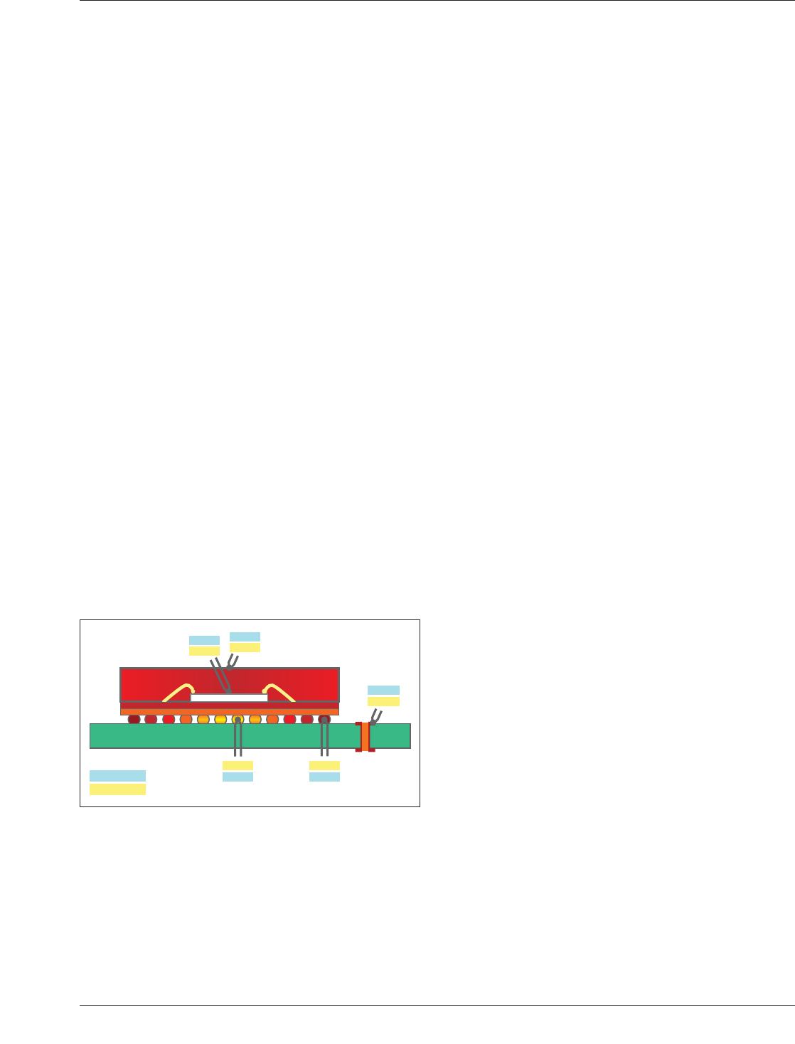
for this is illustrated in Figure 7-3. The optimal reflow pro-
file (temperature vs. time) including the peak temperature
varies with the specific package and the overall assembly.
However, as a guideline, when using SAC305 solder paste
for BGA packages containing SAC305 solder balls, the
minimum peak temperature for moderately complex
PCBAs may need to be not lower than approximately
240°C. When using tin/lead eutectic solder paste for BGA
packages containing SAC305 solder balls, the minimum
peak temperature in most cases can be as low as approxi-
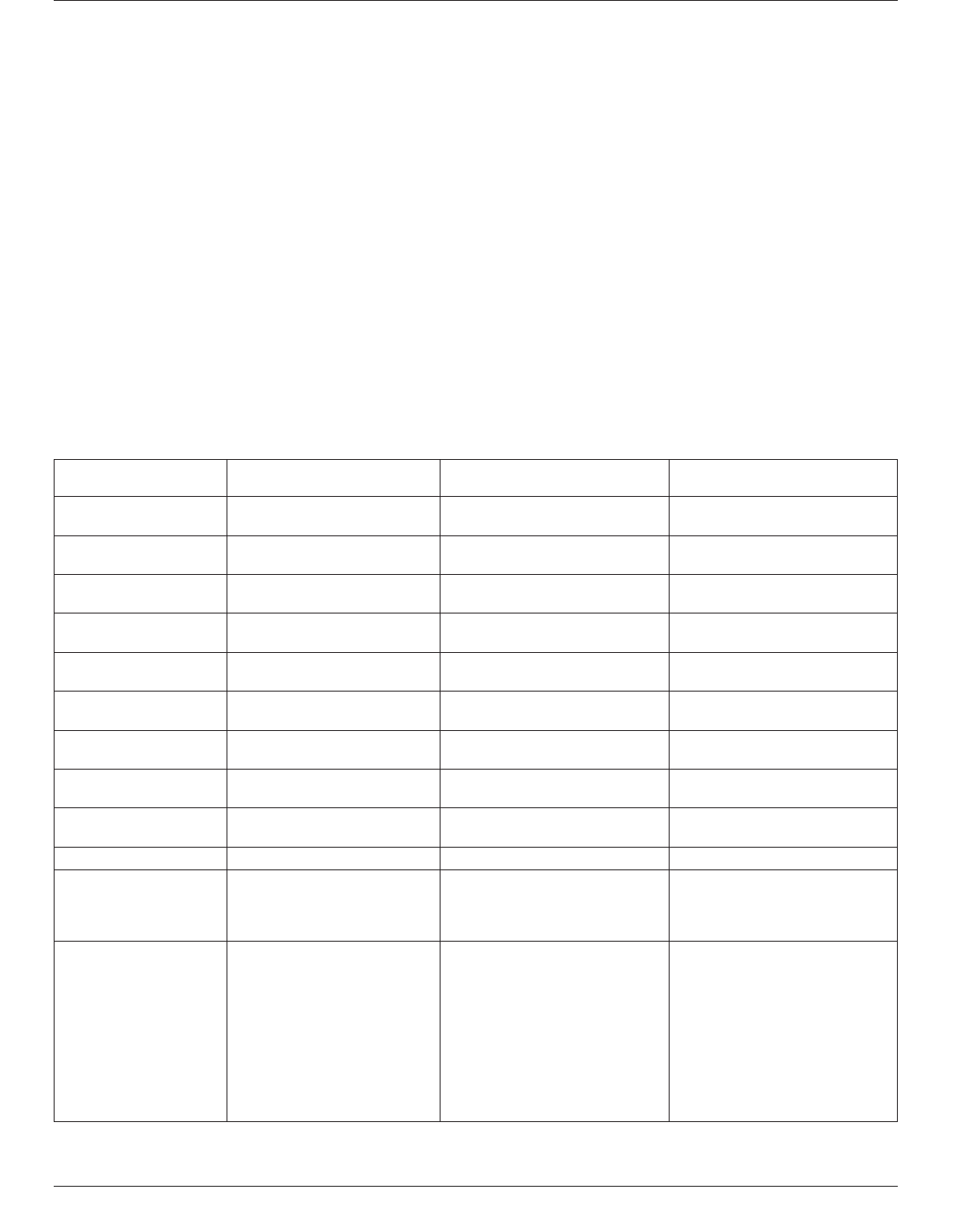
mately 215°C. (See Table 7-3 for recommendations for
proper reflow temperatures.)
Over the years, reflow equipment has changed frequently.
Five design concepts have been used: vapor phase, lamp
infrared (IR), panel IR, and forced gas convection and
diode laser. Vapor phase reflow technology evolved first
and was popular for a few years. Eventually, IR became the
preferred approach. Today, forced gas convection (95% of
total heat source) with IR assist (5% of total heat source)
technology is the method of choice with some applications
requiring an inert oven atmosphere. Diode laser soldering
is the newcomer to the industry and used mostly in high
end high reliability applications such as space, military and
medical industries.
7.1.4.1 Forced Gas Convection Convection heat is
today’s method of choice. Heat is transferred to the printed
circuit assembly (PCA) by low velocity heated gas. Forced
gas convection is a noncontact heating method, with some
heating accomplished by radiation. The rate at which heat
is transferred to the object is directly proportional to the
difference in temperature between the heated gas and the
PCA.
Inline forced gas convection systems have three main sec-
tions: (1) preheat, (2) reflow and (3) cooling. Each section
contains a number of top and bottom zones. The number of
zones has a direct effect on the transport speed and the
user’s ability to fine tune the profile. Adding more zones
allows the user to run a faster belt speed and it permits
more flexibility in accurate profiling. Low volume reflow
systems have three or four zone sections (a zone section
includes top and bottom heaters). Medium volume reflow
systems have five or six zone sections, while the higher
volume systems use seven or more. Typically, a six zone
system will satisfy most reflow requirements, including
very large PCAs and reasonably high transport speeds (up
to 60 cm per minute). Profile changes are accomplished by
adjusting the transport speed and top and bottom tempera-
ture settings.
7.1.4.2 Reflow Atmosphere The atmosphere of the
reflow furnace will affect solder wetting. Reflowing in a
nitrogen environment will result in improved wetting of the
solder joint. This will sometimes allow compensation for
marginally wettable surfaces on the boards as well as oxi-
dized solder balls. In order to obtain the maximum benefit
of the solder paste in a nitrogen environment, it is recom-
mended to monitor the oxygen content and control it within
the limits you have established for your process.
With the migration of products into lead-free technology,
the solderability of the lead-free solder pastes is not as
good as that of tin lead. It is also possible to use up the
activators in the solder paste to clean the oxides off the
paste, land, and balls prior to reflow if paste selection is not
made correctly. This would result in a nonuniform shaped
solder joint and possibly nonwetting of the land. Some sol-
der paste formulations may also be affected by reflow
atmosphere in the formation of voids. When using lead-free
processes with OSP surface finishes, it may be desirable to
reflow the product using nitrogen, especially for hole fill
problems in mixed assemblies. Hole fill problems can be
encountered in lead-free process especially when using no
clean flux and 1
st
or 2
nd
generation OSPs. Use of water
soluble aggressive fluxes and 3
rd
generation OSP should
help minimize hole fill problems.
IPC-7095c-7-3
Figure 7-3 Example of Peak Reflow Temperatures at Vari-
ous Locations at or Near a BGA
220°C
240°C
245°C
for LF-solders
230°C
235°C
260°C
225°C
for Sn/Pb
205°C 217°C
230°C
January 2013 IPC-7095C
79
Copyright IPC-Association Connecting Electronics Industries
Provided by IHS under license with IPC
Not for Resale
No reproduction or networking permitted without license from IHS
--`,,```,,,,````-`-`,,`,,`,`,,`---
Reflowing OSP in nitrogen may also preserve the wettabil-
ity of the lands for downstream processes as well as mini-
mize oxidation of the test points or vias which may have
an impact at in-circuit test (ICT).
7.1.4.3 Time/Temperature Profiles The solder profile,
also known as thermal profile, is one of the key variables
in the manufacturing process that significantly impacts
product yield. Conveyor speed and panel temperatures are
two variables in solder profile development. The solder
profile is not only product specific, it is also flux depen-
dent. Different pastes require different profiles for optimum
performance, so it is important to consult the paste manu-
facturer before developing the solder profile.
For developing the profile, the loaded board is needed for
which the profile is being developed. Start with a given belt
speed and monitor the top-side board temperature using
thermocouples. Most new reflow ovens have built-in
thermocouples and software packages to record the thermal
profile. Also, commercial hardware and software packages,
such as MOLE, data pack and many others are available to
make thermal profile development an easy task. Use of
such profilers has been important in tin/lead assemblies.
Now it is not only important, but critical, that such profil-
ers be used on each product to achieve good yield without
exceeding the temperature constraints imposed by different
types of components. Table 7-3 provides key reflow pro-
files for both tin/lead and lead-free assemblies and also for
mixed assemblies (backward and forward compatibility
profiles). Note that profiles for Lead-free and forward-
compatibility are the same.
With tin/lead, there has been general consensus in the
industry about the composition of solder to be used: eutec-
tic solder with 63% tin and 37% lead composition with
melting point of 183°C. With this composition, there was a
big difference between the melting point (183°C) and peak
temperature (220°C). Even though it has been the recom-
mended practice to maintain the temperature all across the
Table 7-3 Profile Comparison Between SnPb and SAC Alloys
Profile Topic SnPb Alloy Profile
Mixed/Backward
Compatibility Profile
Pb-Free Alloy (SAC 305)/
Forward Compatibility Profile
Alloy Solidus
temperature
183°C 183°C/220°C 217-220°C
Target alloy peak temp
range
210-220°C 228-232°C 235-245°C
Absolute minimum peak
reflow temperature**
205°C 228°C 230°C
Component ramp
up rate
2-4°C/second* 2-4°C/second* 2-4°C/second*
Component ramp down
rate
2-6°C/second* 2-6°C/second* 2-6°C/second*
Soak or preheat
activation temperature
100-180°C* 100-180°C* 140-220°C*
Soak or preheat
activation time
60-120 seconds* 60-120 seconds* 60-150 seconds*
Dwell time above
liquidus
60-90 seconds 60-90 seconds 60-90 seconds
Dwell time at peak
temperature
20 seconds max 20 seconds min 20 seconds max
Solder Paste used Tin/Lead Paste Tin/Lead Paste Lead Free (SAC 305) Paste
SMT component types
All SMT Type Tin/Lead
and Lead Free BUT NOT
Lead Free BGA Balls
All SMT Type Tin/Lead
and Lead Free INCLUDING
SAC Lead Free BGA Balls
ALL COMPONENTS INCLUDING
BGAs are Lead Free including
BGAs with SAC 305
Lead Free BGA balls
Reason for peak
temperatures
Lead Free surface finishes on
BGA Parts have no problem
melting at 205°C. Also all
tin/lead surface finishes have
90% tin any way. Lead Free
finishes have close to 100% tin
with some other lead free
elements like Bismuth
A compromise temperature is
needed so that tin lead parts do
not get overheated and lead free
SAC BGAs with melting point of
220°C can melt, collapse and
fully mix with tin/lead paste.
Lower peak temperatures will
cause SAC BGA balls to either
not melt or partially melt and
increase the incidence of HoP,
Opens and poor reliability
All components are lead free and
can take higher heat. However,
too high a peak temperature may
cause BGA ball drops, opens,
dewetting and board warpage
and Large BGAs are tested
for maximum of 245°C
for MSL level rating
* Verify with the supplier
**Coolest temperature on the board
IPC-7095C January 2013
80
Copyright IPC-Association Connecting Electronics Industries
Provided by IHS under license with IPC
Not for Resale
No reproduction or networking permitted without license from IHS
--`,,```,,,,````-`-`,,`,,`,`,,`---
board between 210-220°C, one could easily get away by
maintaining temperature between 190-225°C, a variation of
almost 35°C and still achieve good reflow soldering results.
In lead-free assembly, the commonly used SAC (Sn, Ag,
and Cu) solders contain 3 to 4% silver, 0.5 to 0.7% copper
and the rest tin. These alloys have the melting point around
220°C. A few components, such as some aluminum elec-
trolytic capacitors, put restrictions on maximum tempera-
ture and duration above 230°C to which they can be sub-
jected. Additional constraints will be dictated by low cost
laminates, plastic connectors and moisture sensitive com-
ponents if used.
To accommodate such constraints, the peak temperature in
lead-free assemblies should be maintained between 230-
245°C, a variation of only 15°C—a tight process window
indeed. This is about a 60% drop from 35°C variation
within tin/lead assemblies as mentioned earlier. The diffi-
culty of achieving a reflow profile to meet the defined pro-
cess window is further increased if large components with
high thermal mass are used on the same board with smaller,
temperature sensitive components. The reasons are simple.
The large components with high thermal mass require a
larger heat input to meet the process window requirements
for Peak Temperature and time above liquidus. However,
this large heat input may result in the smaller, temperature
sensitive components falling outside the process window
requirements. To resolve this issue, very tight process con-
trol and narrow temperature bandwidth across the board is
necessary. Many assembly houses may have a hard time
meeting such requirements, especially on complex boards
without concerted time and effort in developing reflow pro-
files.
The problem can be further compounded by backward
compatibility issues where some lead-free components are
used on a primarily tin/lead board. In such cases, the pro-
file must accommodate both tin/lead and lead-free package
requirements.
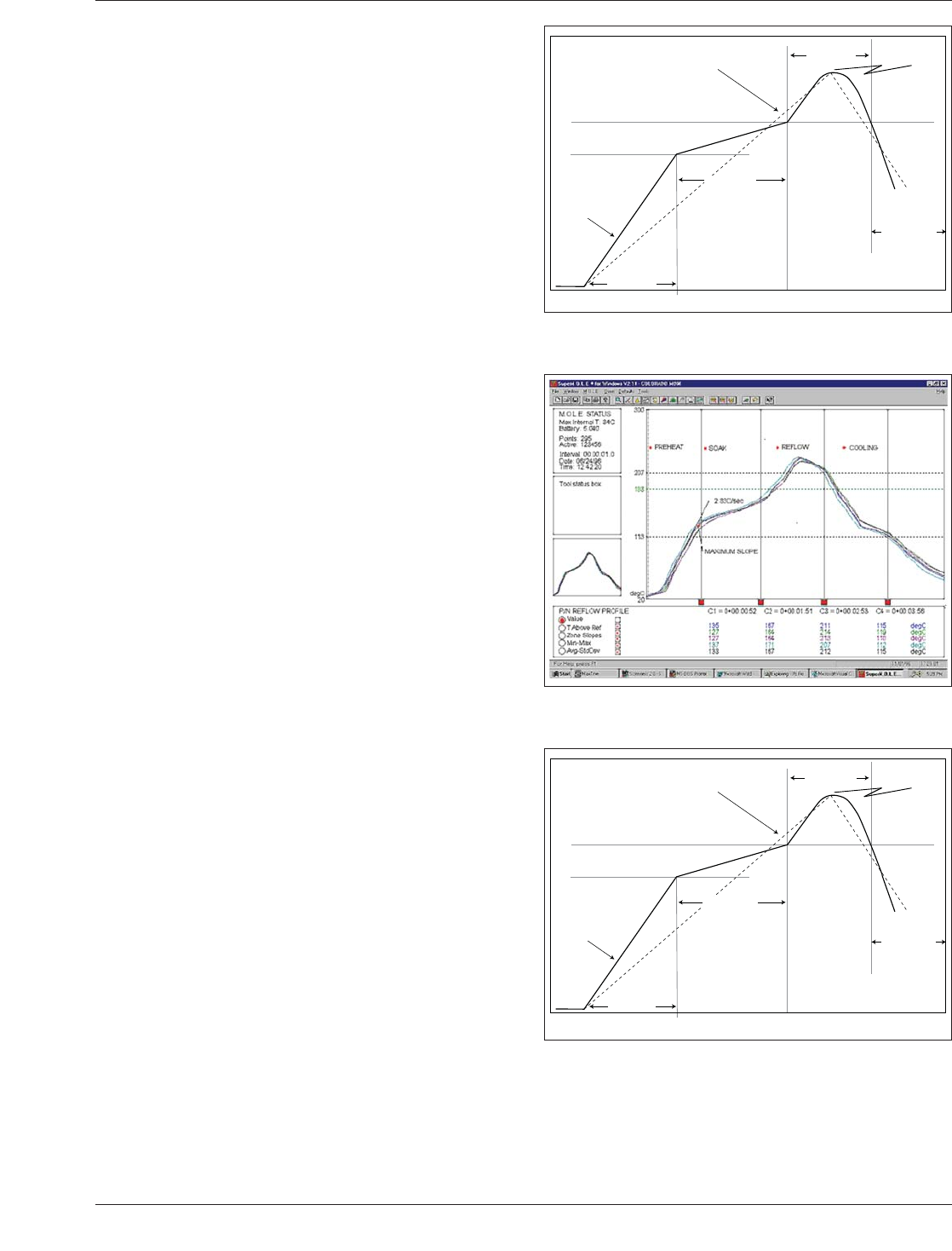
Figures 7-4 to 7-7 show schematic and actual profiles for
tin/lead, lead free, and assemblies with tin/lead and lead-
free components.
7.1.4.4 Preheat Zone The temperature in the preheat
zone can range from 30-175°C and many component sup-
pliers generally recommend 2-4°C/second ramp rate to
avoid thermal shock to sensitive components. Such guide-
lines are considered conservative since some capacitors are
wave soldered where they go from preheat temperature of
about 120°C to wave pot temperature of 260°C. The fast
ramp rate does increase the potential for solder balls and
hence should be kept as low as feasible; however, consid-
eration should be given to the acceptable ramp rate of the
most sensitive component on the assembly.
IPC-7095c-7-4
Figure 7-4 Schematic of Reflow Profile for Tin/Lead
Assemblies
PREHEAT
SOAK
REFLOW
COOLING
210 to 220°C
183°C
Ramp to Peak Profile
with no Soak
100-180°C
Cool Down
4-8°C/Second
60-90 SEC
60-90 SEC
30-60 SEC
for cooling
to room temp
MAX SLOPE
OF 5°C/SEC
90-120 SEC
Figure 7-5 An Example of Tin/Lead Profile with Multiple
Thermocouples
IPC-7095c-7-6
Figure 7-6 Schematic of Reflow Profile for Lead-Free
Assemblies
PREHEAT
SOAK
REFLOW
COOLING
235 to 245°C
217°C
Ramp to Peak Profile
with no Soak
140-220°C
Cool Down
4-8°C/Second
60-90 SEC
60-90 SEC
30-60 SEC
for cooling
to room temp
MAX SLOPE
OF 5°C/SEC
90-120 SEC
January 2013 IPC-7095C
81
Copyright IPC-Association Connecting Electronics Industries
Provided by IHS under license with IPC
Not for Resale
No reproduction or networking permitted without license from IHS
--`,,```,,,,````-`-`,,`,,`,`,,`---