IPC-7095C-2013.pdf - 第56页
has very poor solderability . The wide variation in tin/lead HASL thickness can also cause component coplanarity and solder paste printing problems. The uneven surface makes the solder paste printing task more dif f icul…

(especially OSP). As a general rule, PCBs should be only
be handled by their edges. To achieve maximum shelf life
with any surface finish proper packaging and storage is a
requirement.
5.3.1 Hot Air Solder Leveling (HASL) In this process, the
finished PCB is dipped either vertically or horizontally into
a molten solder bath at about 260°C and the excess solder
is blown away and leveled with hot air, giving the process
its name. HASL is the first heating stress that the PCB
experiences. Any evidence of nonwetting or dewetting is
immediately apparent as the board exits the process.
5.3.1.1 Tin/Lead HASL At one time tin/lead HASL was
the main surface finish solution for PCBs. However, coat-
ing thickness uniformity is a major concern for SMT and
BGA components - the solder thickness varies widely from
0.8 to 0.38 µm. It is generally held that the lower thickness
is not acceptable because the very thin layer of solder is
completely transformed into copper-tin intermetallic, which
Table 5-2 Key Attributes for Various Board Surface Finishes
HASL
SnPb/SnCu OSP
Electroless NI/
Immersion AU
Electrolytic Ni/
Electroplated Au
Immersion
Silver
Immersion
Tin
Shelf Life proper
Handling
1 Year 6-9 Months 1 Year 1 Year 6-9 Months 6 Months
Handling Normal
Avoid
physical
contact
Normal Normal
Avoid
physical
contact
Avoid
physical
contact
SMT land
Surface topology
Domed/
Flatter
Flat Flat Flat Flat Flat
Solderability after
multiple reflow
cycles (2x)
Good, Good Good Good Good Good
Hole fill after multiple
reflow cycles (2x)
Good
May have
problems
after 2x
reflow.
Good Good Good
May have
problems
after 2x
reflow.
Use on thick PCBs
No, holes
difficult
to fill
and clear
Yes
Nickel improves
hole reliability
Nickel improves
holel reliability
yes Yes
Use in thin PCBs
No, prone
to warping
Yes Yes Yes Yes Yes
Solder joint reliability Good Good
BGA
‘‘black pad’’
concerns
Gold
embrittlement
concerns
Planar
microvoid
concerns
Good
Sporadic brittle fracture failure
Card edge contacts
Additional
plating
operation
Additional
plating
operation
Additional
plating
operation
No additional
plating
Additional
plating
operation
Additional
plating
operation
Wire bonding No No No Yes No No
Test point probing Good
Poor,
unless solder
applied during
assembly
Good Good Good Good
Exposed Copper
after Assembly
No
Yes, along
land edges
No No No No
Switches/Contacts No No Yes Yes Yes No
Waste Treatment
and Safety in PCB
Fabrication
Poor/Fair Good Fair Fair Good Good
Process Control
Thickness
control
concerns
Good
Phosphorus
content
concerns
Gold thickness
control
concerns
Good
Thickness
control
concerns
Coating thickness/µm 0.38 - 0.8 0.2 - 0.5 0.05-0.10 0.8 - 2.5 0.07 - 0.10 1.0 - 1.3
General Cost
Comparison
1.0 0.4 - 0.6 2.0 - 3.0 2.0 - 3.0 1.1 - 1.6 1.0 - 1.5
January 2013 IPC-7095C
41
Copyright IPC-Association Connecting Electronics Industries
Provided by IHS under license with IPC
Not for Resale
No reproduction or networking permitted without license from IHS
--`,,```,,,,````-`-`,,`,,`,`,,`---

has very poor solderability. The wide variation in tin/lead
HASL thickness can also cause component coplanarity and
solder paste printing problems. The uneven surface makes
the solder paste printing task more difficult because it is
difficult to achieve a good seal with the stencil. Lack of a
good seal will result in leakage of solder paste beneath the
stencil. The result is more frequent stencil cleaning or an
increased potential for bridging.
Tin/lead HASL is compatible with SMT, BGA and
through-hole components but it is not wire-bondable. It is
compatible with most solder masks. Tin/lead HASL coated
PCBs have a shelf life of 12 months. Typically, it can
withstand 4 to 5 heating cycles without affecting solder-
ability. Tin/lead HASL should only be used with tin/lead
solders.
5.3.1.2 Lead-free HASL Since tin/lead HASL is not
RoHS compliant, there has been a move to lead-free
HASL. The most likely candidates for lead-free HASL are
SnCu (227°C melting point) or SnAgCu (217°C melting
point). The SnAgCu alloy offers the advantage of a lower
melting point and the SnCu alloy offers the advantage of a
lower cost. Some lead-free alloys also add a small amount
of Ni. All high tin alloys are more expensive than the tin/
lead alloy they replace because a low cost material (lead)
is replaced by higher cost materials (tin and silver).
Lead-free HASL is compatible with SMT, BGA, and
through-hole components, but it is not wire-bondable. It is
compatible with most solder masks. Lead-free HASL
coated PCBs have a shelf life of 12 months. Typically, it
can withstand 4 to 5 heating cycles without affecting sol-
derability. Lead-free HASL should only be used with lead-
free solders.
Lead-free HASL is a reasonable alternative for those appli-
cations that need lead-free processing. The finish is smooth
and less domed than tin/lead HASL (see Figure 5-3); how-
ever, coating thickness uniformity is still a concern for
finer pitch components. Lead-free compatible laminates
can tolerate the coating process without significant degra-
dation and without unacceptable warpage (bow and twist).
Very thin boards are still problematic and may require fix-
tures, which is true for any HASL process.
5.3.2 Organic Surface Protection (Organic Solderability
Preservative) OSP Coatings
OSP is an anti-tarnish coat-
ing of an organic compound (such as a benzimidazole-
based compound) which is applied over exposed copper
surfaces to prevent oxidation. An OSP is commonly a
water-based organic compound that selectively bonds with
copper to provide an organometallic layer that protects the
copper, preserving its solderability. Various chemistries of
OSPs are available. Some common ones are benzotriazol,
imidazol and benzimidazol. The coating is commonly
applied either by dipping or spraying. Either method will
work as long as the process is controlled to achieve a uni-
form coating. The coating thickness can range from thin
(0.2 µm) to relatively thick (0.5 µm). Thicker coatings are
preferred if there is a need for multiple reflow cycles
and/or a long wait (24 hour maximum) between soldering
of each side.
OSP coatings are compatible with SMT, BGA and through-
hole components but it is not wire-bondable. Solder mask
compatibility is usually not an issue. OSP coated PCBs
have a shelf life of 6 to 9 months if they are stored prop-
erly. OSP coatings are compatible with tin/lead and lead-
free solders; however, OSP coatings developed specifically
for lead-free soldering must be used.
OSP provides a flat surface which reduces stencil printing
and component coplanarity issues. Since the OSP coated
surface maintains its copper appearance (OSP coating is
transparent), any solder paste misprint is more easily spot-
ted due to increased color contrast. Alcohol or other sol-
vents, if used for washing off the misprinted paste, will
also wash off coatings and, therefore, will increase the risk
of oxidation of the copper which impacts solderability.
However, such boards can be recoated if necessary. Wash-
ing and wiping the board is not recommended, but should
instead be processed in accordance with IPC-7526.
There are some potential process issues with OSP coatings.
Complete hole fill at wave soldering may be difficult to
achieve due to OSP degradation after multiple reflow
cycles, especially when no-clean flux is used. It is a good
idea to use a nitrogen atmosphere during reflow soldering
to limit the amount of degradation. This will reduce the
risk of hole fill problems during wave soldering. It is also
a good idea to have a nitrogen atmosphere over the solder
pot during wave soldering. During reflow soldering, the
solder paste should cover the entire land surface to avoid a
dewetted appearance near the edges; this issue is cosmetic
but it often raises questions. In-circuit test probing may be
a problem because it is difficult to probe through the OSP
coating; test lands should be solder coated (reflow or wave
soldering) to provide a better contact surface.
5.3.3 Noble Platings/Coatings With the RoHS mandate
to remove lead from electronic solder, noble metal coatings
are seeing increased use as PCB surface finishes even
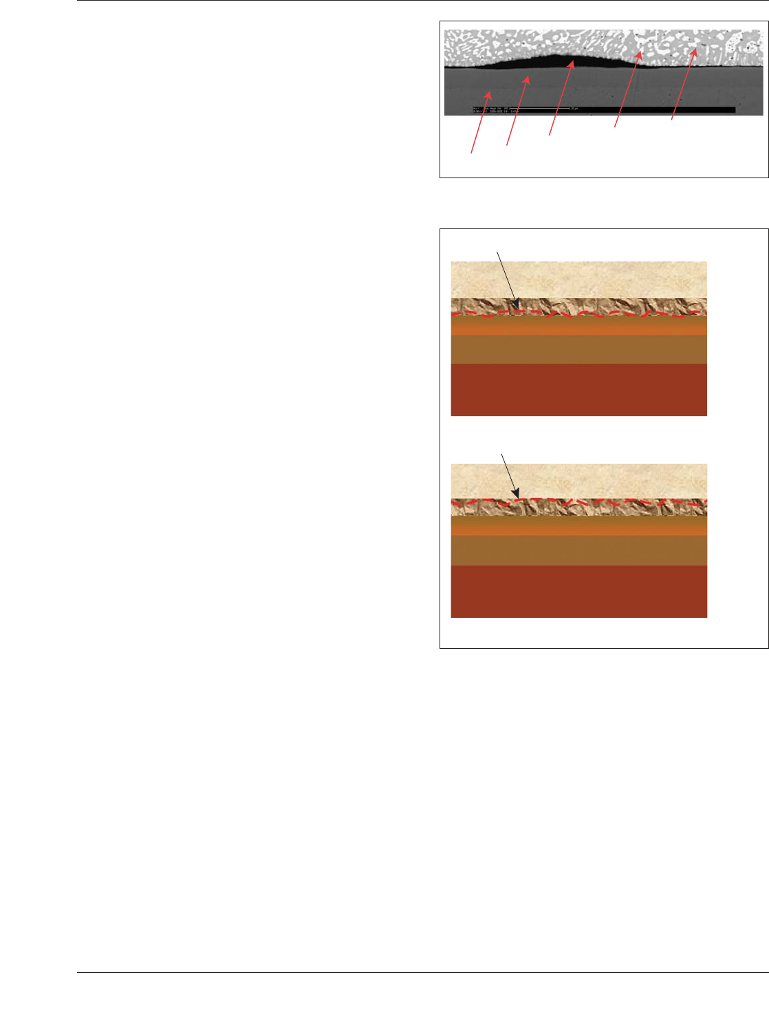
Figure 5-3 Hot Air Solder Level (HASL) Surface Topology
Comparison
IPC-7095C January 2013
42
Copyright IPC-Association Connecting Electronics Industries
Provided by IHS under license with IPC
Not for Resale
No reproduction or networking permitted without license from IHS
--`,,```,,,,````-`-`,,`,,`,`,,`---
though the price of some metals have surpassed historically
high levels. As a result noble coatings typically cost more
than other coatings.
5.3.3.1 Electroless Nickel/Immersion Gold (ENIG) The
electroless nickel/immersion gold surface finish is applied
through the deposition of an initial layer of nickel followed
by a thin, protective layer of gold onto the exposed copper
surfaces of the PCB. The thin layer of immersion gold pre-
serves solderability by preventing oxidation of the highly
active nickel surface. The presence of nickel plating pro-
vides extra strength for the through-hole barrels during
multiple reflow, wave and hand soldering cycles. IPC-
4552, Specification for ENIG Plating, is a valuable refer-
ence document.
ENIG is compatible with SMT, BGA and through-hole
components. It is not considered to be a wire-bondable sur-
face. ENIG coated PCBs have a shelf life of 12 months.
Typically, it can withstand 4 to 5 heating cycles without
affecting solderability. ENIG is compatible with tin/lead
and lead-free solders. It provides a flat surface which
reduces stencil printing and component coplanarity issues.
ENIG application can be performed using a variety of
chemistries, which may lead to different results depending
on the chemistry used. Also, the chemistry and process
may be incompatible with some solder masks. The reduc-
ing agents used in the electroless nickel process contain
either phosphorous or boron. In the reduction of the nickel
in the electroless nickel deposition, either phosphorous or
boron is incorporated into the nickel deposit. The level of
these co-deposited elements should be controlled within the
specified limits. Too much phosphorous or boron variation,
outside the specified limits, may have adverse effects on
solderability and possibly solder joint reliability.
Many companies have used ENIG successfully. However,
when BGAs are used with the electroless nickel/immersion
gold finish the results, at times, can be unpredictable. Two
failure modes have occurred in recent years. The first fail-
ure mode is a nonwetting or dewetting condition referred to
as ‘‘black pad.’’ Figure 5-4 shows the location of crack
constituting a black pad related failure. The failure is
between nickel and Ni-Sn intermetallic (not between the
ball and Ni-Sn intermetallic).
The second failure mode is an interfacial fracture that is
associated with mechanical stress and the failure will occur
between the BGA ball and Ni-Sn intermetallic. Figure 5-5
shows an illustration to highlight the differences between
the two failure modes and the location of their occurrence.
Results from industry consortia and studies by individual
companies suggest that ‘‘black pad’’ is caused by an
aggressive attack (hyperactive corrosion) of the electroless
Ni plating during the immersion Au plating process. The
gold ions from the plating solution attract electrons from
the metallic nickel surface as they plate out as the gold
metal; in return, a nickel ion is released to the bath. Due to
certain microstructure features, such as grain boundaries
and the electrochemistry involved, the exchange does not
always occur locally, i.e., the gold can be deposited to one
feature or area and the nickel ion released from a different
feature or area. The possible consequence of this process is
that selected nickel features become attacked leaving
behind a rough and phosphorous rich layer that forms a
weak bond with solder. The affected solder joints do not
form a robust mechanical bond with the PWB, and as a
result, the solder joints fail with a relatively small applied
force, revealing lands with little or no solder left on them.
The exposed nickel surface on the land is smooth with an
Cu
Ni
Crack
Ni-Sn IMC
BGA Solder Ball
IPC-7095c-5-4
Figure 5-4 Black Pad Related Fracture Showing Crack
Between Nickel & Ni-Sn Intermetallic Layer
Crack Interface
Solder
Ni-Sn IMC
Ni-P
Ni
Cu
(a)
(b)
Solder
Ni-Sn IMC
Ni-P
Ni
Cu
Crack Interface
IPC-7095c-5-5
Figure 5-5 Crack Location for a) Black Pad Related Failure
and (b) Interfacial Fracture When Using ENIG Surface
Finish
January 2013 IPC-7095C
43
Copyright IPC-Association Connecting Electronics Industries
Provided by IHS under license with IPC
Not for Resale
No reproduction or networking permitted without license from IHS
--`,,```,,,,````-`-`,,`,,`,`,,`---