IPC-7095C-2013.pdf - 第77页
IPC-7095c-6-26 Figure 6-26 Heat Pathways to BGA Solder Joint During W ave Soldering A B Heat Pathways to the BGA Solder Joint During Wave Soldering BGA Wave Printed Circuit Board Heat Source C IPC-7095c-6-27 Figure 6-27 …
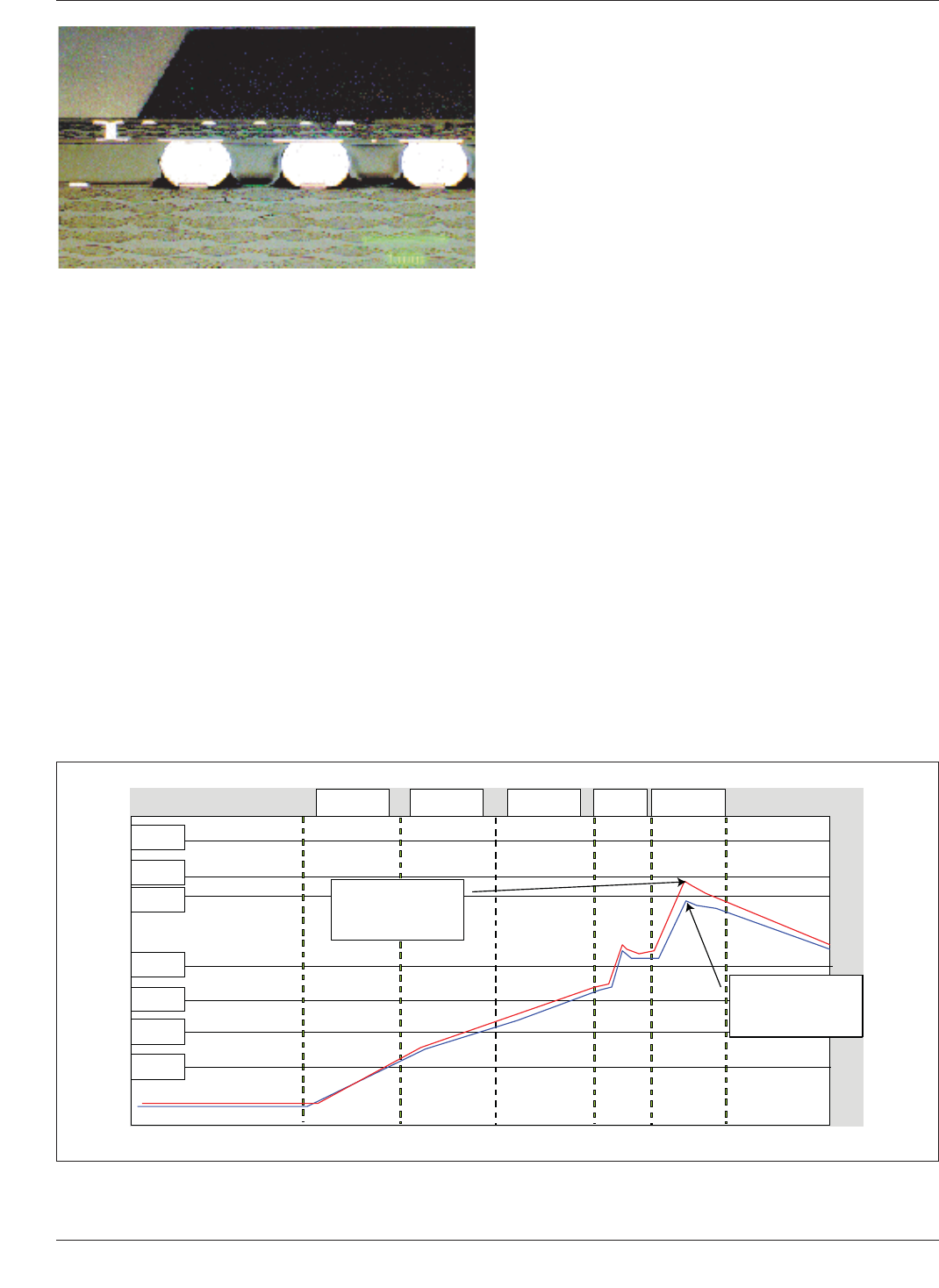
To avoid problems in BGA solder joints on the top side of
the board, their temperatures should not exceed 150°C dur-
ing tin/lead wave soldering and 190°C for lead-free alloy
wave soldering. This is less than the maximum temperature
allowed for the fine pitch leaded components such as plas-
tic QFPs.
Figure 6-25 is an example of an acceptable temperature
profile for the solder joints on a mixed technology board
during the wave solder process.
To determine the various ways of keeping the temperature
below 150°C (or 190°C for lead free), it is best to first
identify the various ways in which the BGA solder joints
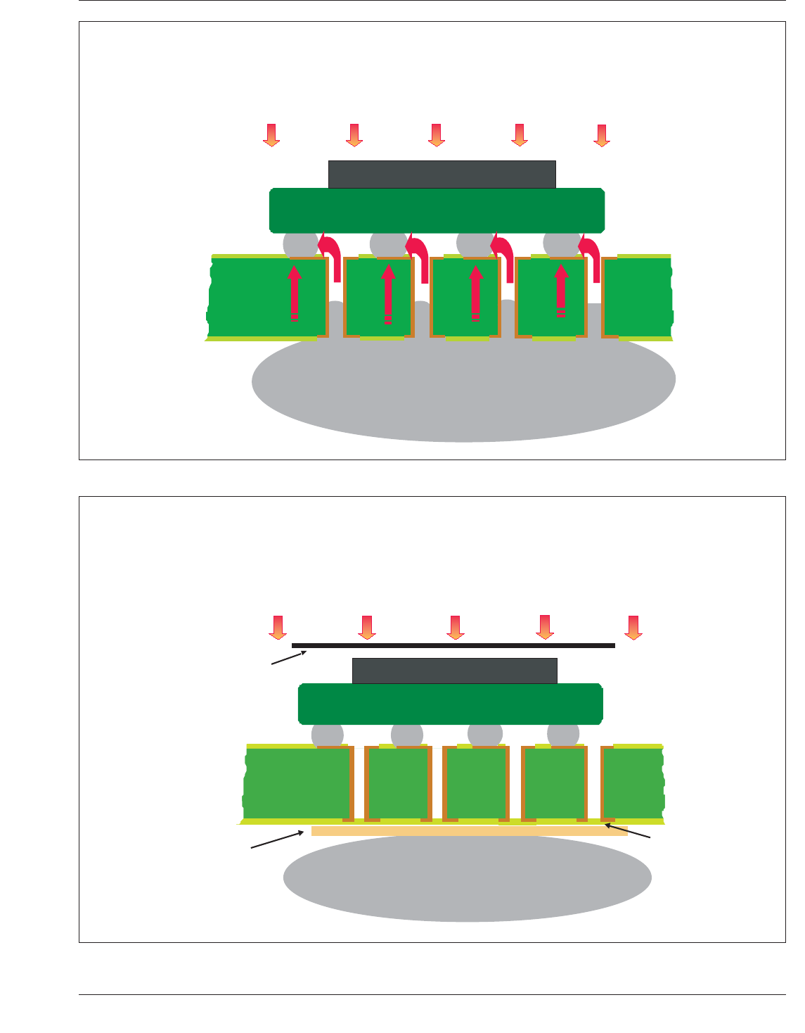
are heated during the wave solder process. Figure 6-26
illustrated three pathways. Pathway A is by conduction
through the thickness of the board from bottom to top.
Pathway B is by conduction through the barrel of the via,
along a conductor connecting the via to the BGA solder
joint land. Pathway C is by convection and radiation from
the preheaters on the top in the wave solder machine.
6.4.3 Methods of Avoiding Top Side Reflow The meth-
ods of avoiding top side reflow aim to reduce the heat
transfer to the BGA solder joints by one or more of the
three pathways described above. Figure 6-27 illustrates
these methods. A heat shield can be placed over the BGA
packages to avoid direct heating from the preheaters in the
wave solder machine. These shields can be mechanically
attached to the wave solder pallets.
Secondly, vias can be capped by solder mask on the bottom
side of the board. This via-capping process is very com-
monly employed in the industry, for a variety of reasons.
Via capping rules should be built into the design for manu-
facturability (DfM) process, during board design.
Vias that certainly need to be capped are those that are
connected to the BGA land with a short trace length or
those that are connected to a plane in the board.
Thirdly, a nonmetallic wave shield can be placed immedi-
ately below the BGA package locations on the bottom side
of the board to avoid the wave from touching these board
locations. The wave shield can also be attached to the wave
pallet by nonmetallic fingers.
Selective wave pallets can utilize solid material under the
BGAs to prevent solder contact with the bottom of the
board and heat transfer up the vias to the lands. This will
prevent secondary reflow of the BGA joints.
The efficacy of each of these methods should be confirmed
by measuring the temperature profile of the BGA solder
joints during the wave solder process and ensuring that
they stay below 150°C.
Figure 6-24 Example of Top Side Reflow Joints
IPC-7095c-6-25
Figure 6-25 Example of Wave Solder Temperature Profile of Topside of Mixed Component Assembly
150° C
160° C
183°C
80° C
Zone # 2
100° C
Zone # 1 Zone # 3 Chip Contour
40° C
60° C
Maximum peak
temperature for
BGA is 150°
C
Maximum peak
temperature for
Fine Pitch is 160°C
IPC-7095C January 2013
62
Copyright IPC-Association Connecting Electronics Industries
Provided by IHS under license with IPC
Not for Resale
No reproduction or networking permitted without license from IHS
--`,,```,,,,````-`-`,,`,,`,`,,`---
IPC-7095c-6-26
Figure 6-26 Heat Pathways to BGA Solder Joint During Wave Soldering
A
B
Heat Pathways to the BGA Solder Joint During Wave Soldering
BGA
Wave
Printed
Circuit
Board
Heat Source
C
IPC-7095c-6-27
Figure 6-27 Methods of Avoiding BGA Topside Solder Joint Reflow
Methods of Avoiding Topside BGA Solder
Joint Reflow During Wave Soldering
BGA
Wave
Printed
Circuit
Board
Heat Shield
(Attached to Pallet)
Nonmetallic
Wave Shield
(Attached to Pallet)
Via Capping
Heat Source
January 2013 IPC-7095C
63
Copyright IPC-Association Connecting Electronics Industries
Provided by IHS under license with IPC
Not for Resale
No reproduction or networking permitted without license from IHS
--`,,```,,,,````-`-`,,`,,`,`,,`---
6.4.4 Top Side Reflow for Lead-Free Boards Most lead-
free solders targeted for use, including the popular solders
in the SnAgCu system, have melting points higher than
that for eutectic tin/lead solder. Hence, the potential for top
side reflow when wave soldering boards with surface
mount lead-free components already reflow soldered on the
top side of the board is significantly reduced. For SnAgCu
solders, the maximum top side solder joint reflow tempera-
ture can reach 190°C without any impact on the BGA sol-
der joints.
6.5 Testability and Test Point Access The differences
in contact design have differing effects on the quality and
reliability of the contact, contactability, and later solder-
ability. The effects are negligible and insignificant when the
contact is minimal.
6.5.1 Component Testing As the BGA pitches and sol-
der ball size decrease, socket manufacturers face increasing
challenges in the design of sockets to adequately test BGA
packages. There are a myriad of tip designs socket manu-
facturers are working with to meet the needs of sub-mm
pitch BGAs.
One challenge is to be able to make contact to all BGA
individual balls. While attaching to a PCB, the solder balls
melt and self align to attach to the corresponding lands on
the PCB. Therefore, wider variations in the placements of
solder balls are tolerable with respect to BGA attach to the
PCB. But these variations need to be tightened in the case
of test and burn-in and thus there is no self-alignment of
solder balls to socket contacts.
The design of socket probes needs to take into account the
solder ball height variation. A larger variation in solder ball
height would require a wider reach range for socket probes,
and also when testing, the solder balls will be more vulner-
able. Burn-in of BGAs is conducted at an elevated tem-
perature. The burn-in time/temperature combination will
soften the solder balls to an extent dependent upon the sol-
der ball material. Under test probe pressure, the softened
solder ball will deform heavily and may affect the contact
quality during burn-in. The socket manufacturers need to
assure that the probes do not stick to softened solder balls
and the solder balls are not pulled away.
The socket test probe design is also critical in that the
probe does not gouge the solder ball in such a way or to
such an extent that the deformation becomes a quality or
reliability concern during or after BGA attach to the PCB.
Some contacts touch the solder ball on their sides, and
some on the tip of the solder balls. In some designs, the
individual pins are spring-loaded; in others, all contact
probes are in the same rigid plane.
6.5.2 Damage to the Solder Balls During Test and Burn-
In
In their pristine form, eutectic solder balls on a BGA
are shiny and quite round. Their attach, handling, and
subsequent BGA processing steps may induce deformation,
damage, pokes and dents.
The solder ball deformation during test and burn-in is an
expected phenomenon and, as such, is an acceptable
anomaly as long as it does not affect the usefulness of the
product. Many contact designs exist, each vying for a bet-
ter share of the market. Each contact will impart its unique
imprint on the solder ball. These probes contact the solder
ball at differing locations and impart unique imprints char-
acteristic of the contact design to the solder ball during test
and burn-in.
Solder balls have been known to come off in certain situa-
tions. Rather than trying to catch the problem by using
vision systems to detect the presence or absence of solder
balls or the damage to solder balls during testing, it is pru-
dent to optimize the solder attachment and to choose a test
socket which is benign to the device under test.
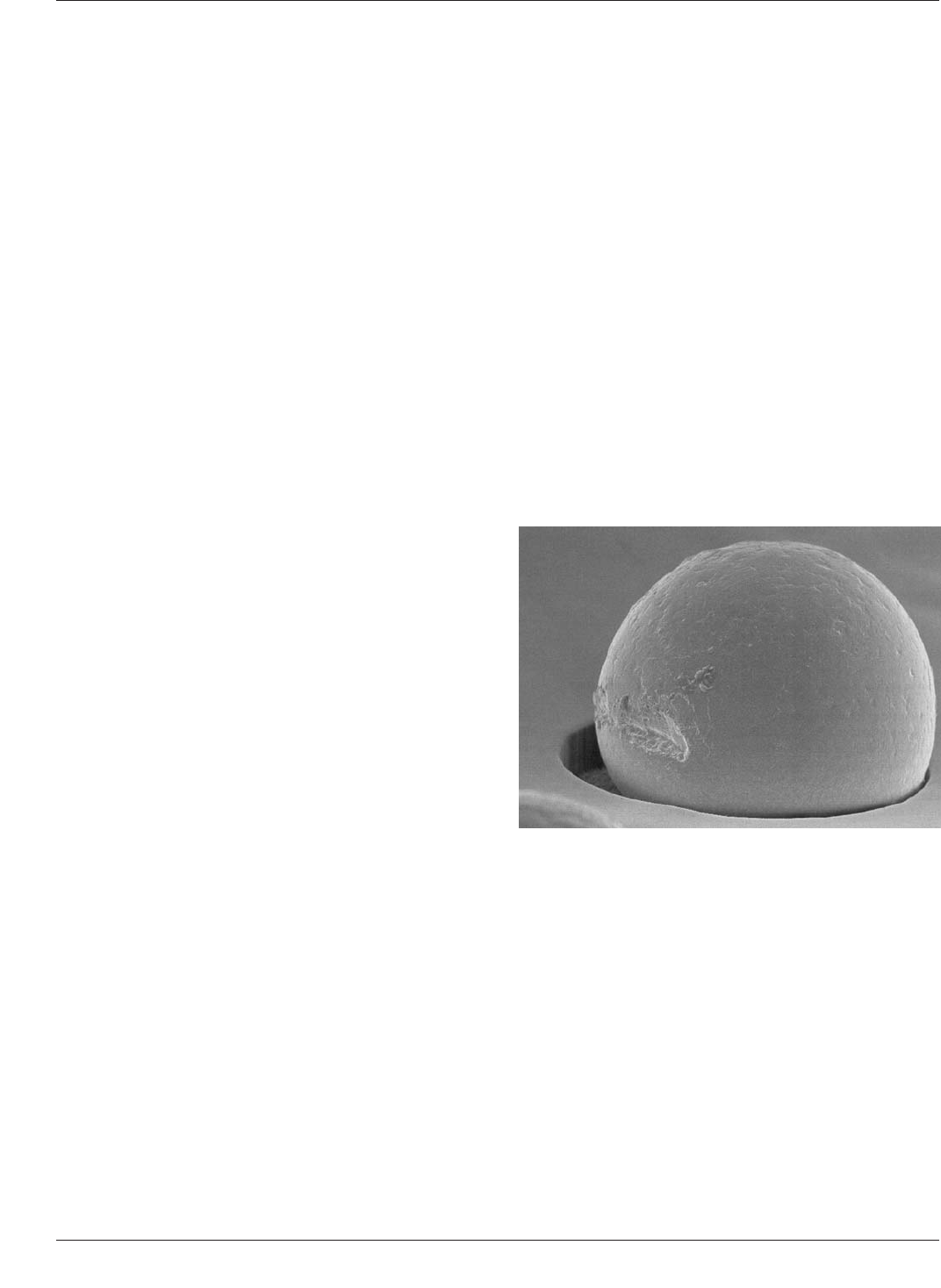
Some contacts disturb only the sides of the solder ball and
not the bottom. The bottom of the solder ball is untouched
during contact. One such example is shown in Figure 6-28.
Other contacts impact the bottom of the solder ball. Figure
6-29 shows a solder ball which has been contacted at the
bottom of the solder ball. The concern is that, during
reflow, flux may get entrapped in the depressions formed
by the contact and may explode under reflow heat, splatter-
ing solder around, causing shorts, etc.
Some contacts are designed not to allow the entrapment of
flux. Contact probes may contact the bottom of a solder
ball to create a pattern which provides a path for the flux
to escape and will not entrap flux during reflow.
Other contact impressions allow the entrapment of flux. If
the impressions cause a hole at the bottom of the solder
ball then there is a greater chance of flux entrapment. Such
entrapment may be quite benign for shallow depressions.
Figure 6-28 An Example of a Side Contact Made with a
Tweezers Type Contact
IPC-7095C January 2013
64
Copyright IPC-Association Connecting Electronics Industries
Provided by IHS under license with IPC
Not for Resale
No reproduction or networking permitted without license from IHS
--`,,```,,,,````-`-`,,`,,`,`,,`---