IPC-7095C-2013.pdf - 第167页
T able A-2 Corrective Action Indicator for Lands used with 0.8, 0.65 or 0.5 mm Pitch Vo i d T ype V oid Description Corrective Action Indicator Action T aken Class 1 Class 2 Class 3 Determined by cross section/X-ray lami…
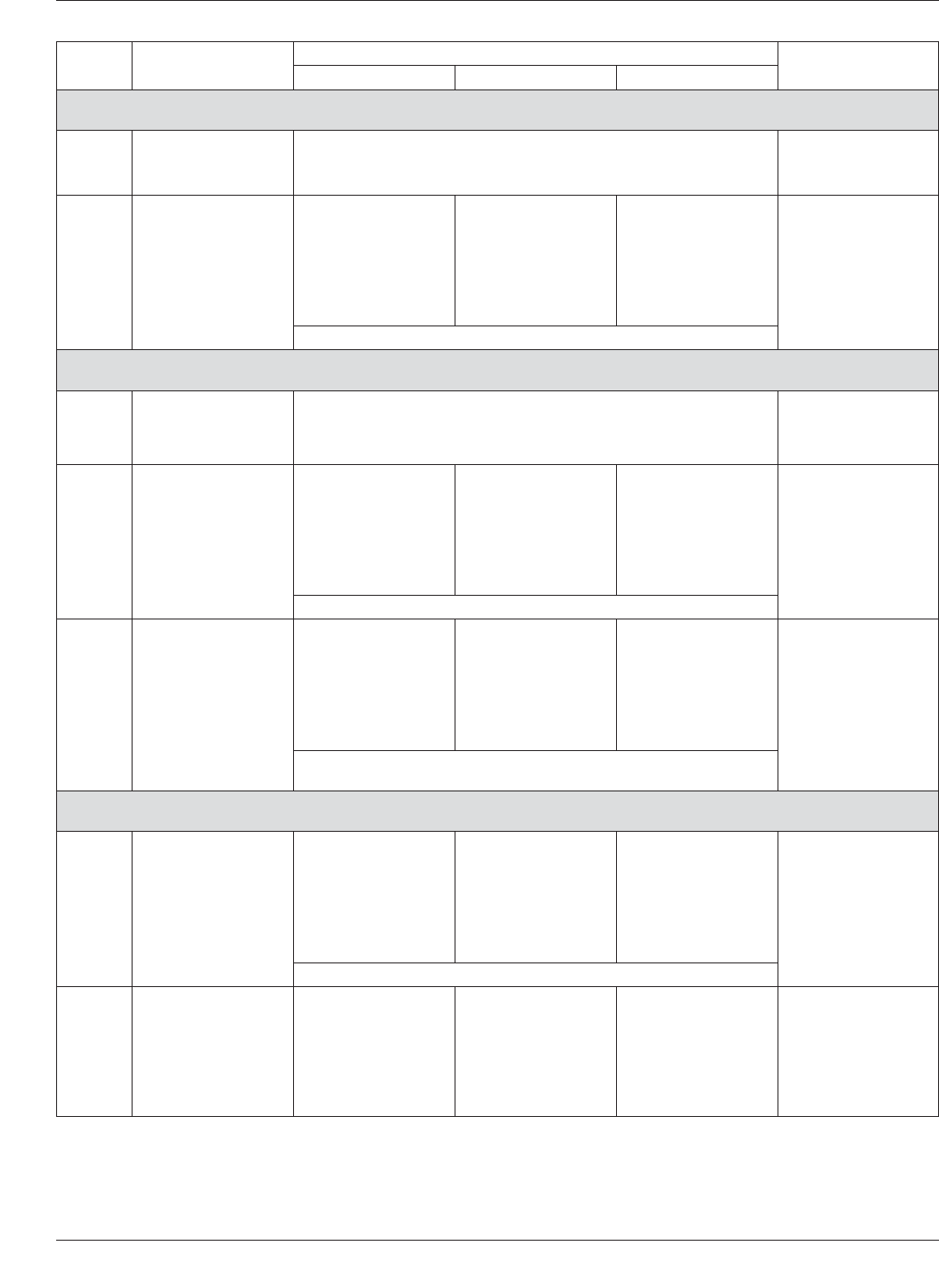
Table A-1 Corrective Action Indicator for Lands used with 1.5, 1.27 or 1.0 mm Pitch
Void
Type Void Description
Corrective Action Indicator
Action TakenClass 1 Class 2 Class 3
Determined by cross section/X-ray laminography
(sampling according to Section 7.6.3) at Component Incoming Evaluation
A Voids within the
solder ball (prior
to assembly)
Up to 90% balls may have voids
Maximum Void size in any ball is 20% of Area
(45% of the image diameter)
Investigate root
cause in process &
take corrective action
B Voids at package
interface (prior to
assembly)
Up to 80% balls may
have voids
Maximum Void size
in any ball is 15% of
area
(40% of the image
diameter)
Up to 70% balls may
have voids
Maximum Void size
in any ball is 10% of
area
(32% of the image
diameter)
Up to 50% balls may
have voids
Maximum Void size in
any ball is 5% of area
(22% of the image
diameter)
Investigate root
cause in process &
take corrective action
All balls with cumulative voids no matter what size are considered
Determined by cross section/X-ray laminography
(sampling according to Section 7.6.3) Evaluation after Assembly
C Voids within the ball
after PCA reflow
Up to 100% balls may have voids
Maximum Void size in any ball is 25% of Area
(50% of the image diameter)
Investigate root
cause in process &
incoming parts, take
corrective action
D Voids at the package
interface after PCA
reflow
Up to 100% balls
may have voids
Maximum Void size
in any ball is 25% of
area
(50% of the image
diameter)
Up to 80% balls may
have voids
Maximum Void size
in any ball is 20% of
area
(45% of the image
diameter)
Up to 60% balls may
have voids
Maximum Void size
in any ball is 15% of
area
(40% of the image
diameter)
Investigate root
cause in process &
incoming parts, take
corrective action
All balls with cumulative voids no matter what size are considered
E Voids at the mounting
surface interface after
PCA reflow
Up to 100% balls
may have voids
Maximum Void size
in any ball is 25% of
area
(50% of the image
diameter)
Up to 80% balls may
have voids
Maximum Void size
in any ball is 20% of
area
(45% of the image
diameter)
Up to 60% balls may
have voids
Maximum Void size
in any ball is 15% of
area
(40% of the image
diameter)
Investigate root
cause in process &
incoming parts, take
corrective action
Balls with cumulative voids smaller than 2% of the area (15% of the
image diameter) are not counted
Determined by transmission X-ray (sampling according to Section 7.6.3)
for Process Evaluation either at Component Incoming or after Assembly
A, B Voids at incoming Up to 80% balls may
have voids
Maximum Void size
in any ball is 15% of
area
(40% of the image
diameter)
Up to 70% balls may
have voids
Maximum Void size
in any ball is 10% of
area
(32% of the image
diameter)
Up to 50% balls may
have voids
Maximum Void size in
any ball is 5% of area
(22% of the image
diameter)
Investigate root
cause in process &
take corrective action.
All balls with cumulative voids no matter what size are considered
C, D, E Voids after PCA
reflow
Up to 70% balls may
have voids
Maximum Void size
in any ball is 25% of
area
(50% of the image
diameter)
Up to 60% balls may
have voids
Maximum Void size
in any ball is 25% of
area
(50% of the image
diameter)
Up to 50% balls may
have voids
Maximum Void size
in any ball is 20% of
area
(45% of the image
diameter)
Investigate root
cause in process &
incoming parts, take
corrective action
IPC-7095C January 2013
152
Copyright IPC-Association Connecting Electronics Industries
Provided by IHS under license with IPC
Not for Resale
No reproduction or networking permitted without license from IHS
--`,,```,,,,````-`-`,,`,,`,`,,`---
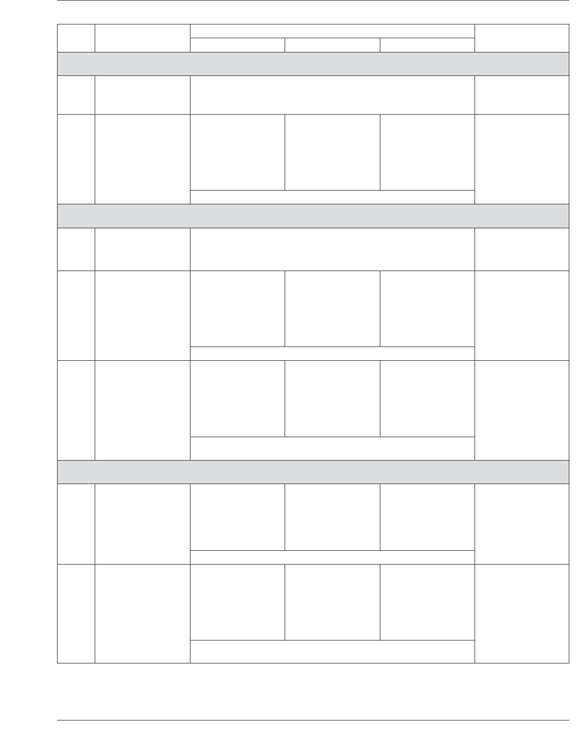
Table A-2 Corrective Action Indicator for Lands used with 0.8, 0.65 or 0.5 mm Pitch
Void
Type Void Description
Corrective Action Indicator
Action TakenClass 1 Class 2 Class 3
Determined by cross section/X-ray laminography
(sampling according to Section 7.6.3) at Component Incoming Evaluation
A Voids within the
solder ball (prior
to assembly)
Up to 90% balls may have voids
Maximum Void size in any ball is 15% of Area
(40% of the image diameter)
Investigate root
cause in process &
take corrective action
B Voids at package
interface (prior to
assembly)
Up to 80% balls may
have voids
Maximum Void size
in any ball is 12% of
area
(35% of the image
diameter)
Up to 70% balls may
have voids
Maximum Void size in
any ball is 9% of area
(30% of the image
diameter)
Up to 50% balls may
have voids
Maximum Void size in
any ball is 4% of area
(20% of the image
diameter)
Investigate root
cause in process &
take corrective action
All balls with cumulative voids no matter what size are considered
Determined by cross section/X-ray laminography
(sampling according to Section 7.6.3) Evaluation after Assembly
C Voids within the ball
after PCA reflow
Up to 100% balls may have voids
Maximum Void size in any ball is 20% of Area
(45% of the image diameter)
Investigate root
cause in process &
incoming parts, take
corrective action
D Voids at the package
interface after PCA
reflow
Up to 100% balls may
have voids
Maximum Void size
in any ball is 20% of
area
(45% of the image
diameter)
Up to 80% balls may
have voids
Maximum Void size
in any ball is 15% of
area
(40% of the image
diameter)
Up to 60% balls may
have voids
Maximum Void size
in any ball is 12% of
area
(35% of the image
diameter)
Investigate root
cause in process &
incoming parts, take
corrective action
All balls with cumulative voids no matter what size are considered
E Voids at the mounting
surface interface after
PCA reflow
Up to 100% balls may
have voids
Maximum Void size in
any ball is 20% of
area
(45% of the image
diameter)
Up to 80% balls may
have voids
Maximum Void size in
any ball is 15% of
area
(40% of the image
diameter)
Up to 60% balls may
have voids
Maximum Void size in
any ball is 12% of
area
(35% of the image
diameter)
Investigate root
cause in process &
incoming parts, take
corrective action
Balls with cumulative voids smaller than 2% of the area (15% of the
image diameter) are not counted
Determined by transmission X-ray (sampling according to Section 7.6.3)
for Process Evaluation either at Component Incoming or after Assembly
A, B Voids at incoming Up to 80% balls may
have voids
Maximum Void size in
any ball is 9% of area
(30% of the image
diameter)
Up to 70% balls may
have voids
Maximum Void size in
any ball is 6% of area
(25% of the image
diameter)
Up to 50% balls may
have voids
Maximum Void size in
any ball is 4% of area
(20% of the image
diameter)
Investigate root
cause in process &
take corrective action
All balls with cumulative voids no matter what size are considered
C, D, E Voids after PCA
reflow
Up to 70% balls may
have voids
Maximum Void size
in any ball is 20% of
area
(45% of the image
diameter)
Up to 60% balls may
have voids
Maximum Void size
in any ball is 15% of
area
(40% of the image
diameter)
Up to 50% balls may
have voids
Maximum Void size
in any ball is 10% of
area
(32% of the image
diameter)
Investigate root
cause in process &
incoming parts, take
corrective action
Balls with cumulative voids smaller than 4% of the area (20% of the
image diameter) are not counted
January 2013 IPC-7095C
153
Copyright IPC-Association Connecting Electronics Industries
Provided by IHS under license with IPC
Not for Resale
No reproduction or networking permitted without license from IHS
--`,,```,,,,````-`-`,,`,,`,`,,`---
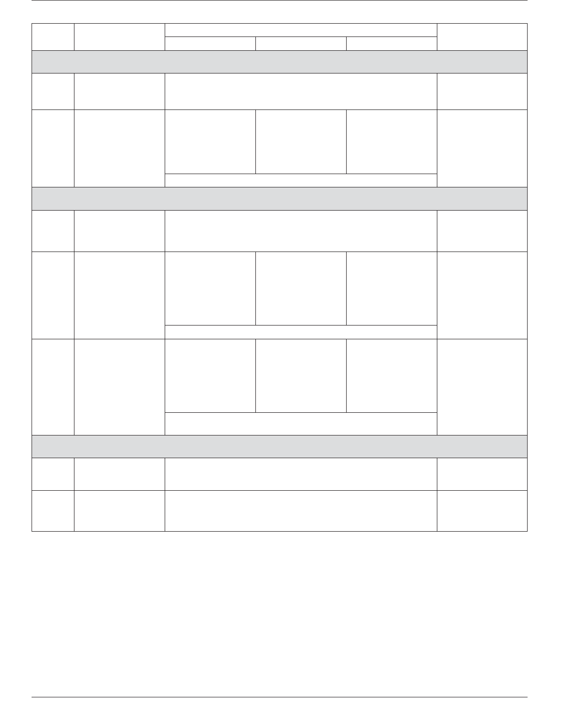
Table A-3 Corrective Action Indicator for Microvia in Pad Lands used with 0.5, 0.4 or 0.3 mm Pitch
Void
Type Void Description
Corrective Action Indicator
Action TakenClass 1 Class 2 Class 3
Determined by cross section/X-ray laminography
(sampling according to Section 7.6.3) at Component Incoming Evaluation
A Voids within the
solder ball (prior
to assembly)
Up to 90% balls may have voids
Maximum Void size in any ball is 9% of Area
(30% of the image diameter)
Investigate root
cause in process &
take corrective action
B Voids at package
interface (prior to
assembly)
Up to 80% balls may
have voids
Maximum Void size in
any ball is 6% of area
(25% of the image
diameter)
Up to 70% balls may
have voids
Maximum Void size in
any ball is 4% of area
(20% of the image
diameter)
Up to 50% balls may
have voids
Maximum Void size in
any ball is 2% of area
(15% of the image
diameter)
Investigate root
cause in process &
take corrective action
All balls with cumulative voids no matter what size are considered
Determined by cross section/X-ray laminography
(sampling according to Section 7.6.3) Evaluation after Assembly
C Voids within the ball
after PCA reflow
Up to 100% balls may have voids
Maximum Void size in any ball is 25% of Area
(50% of the image diameter)
Investigate root
cause in process &
incoming parts, take
corrective action
D Voids at the package
interface after PCA
reflow
Up to 100% balls
may have voids
Maximum Void size
in any ball is 15% of
area
(40% of the image
diameter)
Up to 80% balls may
have voids
Maximum Void size
in any ball is 10% of
area
(32% of the image
diameter)
Up to 60% balls may
have voids
Maximum Void size in
any ball is 5% of area
(22% of the image
diameter)
Investigate root
cause in process &
incoming parts, take
corrective action
All balls with cumulative voids no matter what size are considered
E Voids at the mounting
surface interface after
PCA reflow
Up to 100% balls
may have voids
Maximum Void size
in any ball is 15% of
area
(40% of the image
diameter)
Up to 80% balls may
have voids
Maximum Void size
in any ball is 10% of
area
(32% of the image
diameter)
Up to 60% balls may
have voids
Maximum Void size in
any ball is 5% of area
(22% of the image
diameter)
Investigate root
cause in process &
incoming parts, take
corrective action
Balls with cumulative voids smaller than 2% of the area (15% of the
image diameter) are not counted
Determined by transmission X-ray (sampling according to Section 7.6.3)
for Process Evaluation either at Component Incoming or after Assembly
A, B Voids at incoming Not Recommended Investigate root
cause in process &
take corrective action
C, D, E Voids after PCA
reflow
Not Recommended Investigate root
cause in process &
incoming parts, take
corrective action
Note: If a board design or manufacturing does not include filling vias, a joint team between the designer, customer, material supplier, and assembly engineering
should be formed to conduct experiments to minimize voiding. Once the voiding has been minimized, an acceptable level of voiding for that specific product
should be established and used for process control for that product.
IPC-7095C January 2013
154
Copyright IPC-Association Connecting Electronics Industries
Provided by IHS under license with IPC
Not for Resale
No reproduction or networking permitted without license from IHS
--`,,```,,,,````-`-`,,`,,`,`,,`---