IPC-7095C-2013.pdf - 第60页
the PCB. An organic substance is deposited as part of the process; this reduces the oxidation that would be expected with a pure silver surface. IPC-4553 Specification for Immersion Silver Plating is a valuable reference …
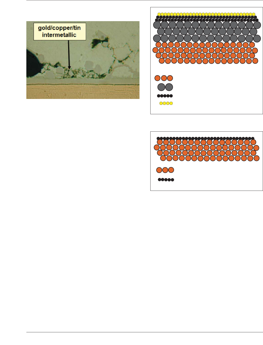
the solder joints. Gold embrittlement creates weak solder
joints that will eventually fail (see Figure 5-8).
5.3.3.3 Electroless Nickel/Electroless Palladium/
Immersion Gold (ENEPIG)
The electroless nickel/
electroless palladium/immersion gold process is similar to
ENIG except it uses a palladium metal layer that is depos-
ited after the nickel layer prior to the final gold layer. The
palladium layer is much harder than gold, providing added
strength to the surface finish for wire-bonding while pro-
tecting the underlying nickel from oxidation. The ENEPIG
structure is illustrated in Figure 5-9. ENEPIG is not widely
available from PCB suppliers and it is not widely used by
PCBA assemblers.
This finish is compatible with SMT, BGA and through-hole
components and it is wire-bondable. Nickel/gold finishes
typically can withstand 4 to 5 heating cycles without
affecting solderability. ENEPIG-coated PCBs have a shelf
life of 12 months. It provides a flat surface which reduces
stencil printing and component coplanarity issues. The high
plating temperatures and low pH of the nickel/palladium/
gold plating process can be incompatible with some solder
masks.
ENEPIG is best suited for lead-free soldering. Studies have
shown that ENEPIG does not produce very reliable tin/lead
solder joints. Pd cannot form an alloy with lead. The non-
alloyed lead disrupts the IMC formation. As Pd is intro-
duced into the Ni3Sn4 layer, it aggregates into distinctive
clusters (away from lead) creating a nonuniform IMC
layer. The excessive growth and lack of uniformity of the
IMC leads to poor reliability when ENEPIG is used with
tin/lead solder.
5.3.3.4 Direct Immersion Gold (DIG) DIG is a finishing
process that can directly deposit gold onto the copper sur-
face by utilizing an electroless plating process. A graphic
representation is shown in Figure 5-10. It is possible to
directly deposit gold on the copper surface with excellent
coverage. The main gold depositing reaction is an auto-
catalytic rather than displacement. Solderability is good
when the gold film thickness is within the range of 30 to
80 nm; however, underlying copper roughness can affect
solder wetting. Good wire-bonding characteristics can also
be derived from deposits plated by a neutral pH, auto-
catalytic type heavy electroless gold plating bath on top of
the flash gold. DIG is not widely available from PCB sup-
pliers, and it is not widely used by PCBA assemblers.
DIG typically can withstand 3 to 4 heating cycles without
affecting solderability. Solder mask compatibility is usually
not an issue. DIG coated PCBs have a shelf life of 9 to 12
months. It provides a flat surface which reduces stencil
printing and component coplanarity issues. DIG may be
best suited for tin/lead soldering applications (one reason it
is not widely used). Lead-free solder results are usually
inferior (in terms of solderability and wetting) compared to
tin/lead solder.
5.3.3.5 Immersion Silver The immersion silver finish is
produced by the selective displacement of copper atoms
with silver atoms on the exposed metal (copper) surface of
Figure 5-8 Gold Embrittlement
Copper Surface Cleaned and Microetched
Electroless Ni 5 µm (200 microinches)
Electroless Pd 0.06 µm (2.4 microinches)
Immersion Au 0.03 µm (1.2 microinches)
IPC-7095c-5-9
Figure 5-9 Graphic Depiction of Electroless Nickel/
Electroless Palladium/Immersion Gold
Copper Surface Cleaned and Microetched
Immersion Gold 0.06 µm (2 microinches)
IPC-7095c-5-10
Figure 5-10 Graphic Depiction of Directed Immersion
Gold
January 2013 IPC-7095C
45
Copyright IPC-Association Connecting Electronics Industries
Provided by IHS under license with IPC
Not for Resale
No reproduction or networking permitted without license from IHS
--`,,```,,,,````-`-`,,`,,`,`,,`---
the PCB. An organic substance is deposited as part of the
process; this reduces the oxidation that would be expected
with a pure silver surface. IPC-4553 Specification for
Immersion Silver Plating is a valuable reference document.
Immersion silver finishes are compatible with SMT, BGA
and through-hole components but it is not wire-bondable.
Silver finishes are compatible with most solder masks.
Immersion silver PCBs have a shelf life of 6 to 9 months
if they are stored properly. It provides a flat surface which
reduces stencil printing and component coplanarity issues.
During soldering, the silver dissolves into the solder and
becomes part of the solder joint; it is almost undetectable
in the final solder joint. Since the silver dissolves during
soldering, the solder joins directly to the copper surface.
Immersion silver finishes typically can withstand 4 to 5
heating cycles without affecting solderability. Immersion
silver is compatible with tin/lead and lead-free solders.
Immersion silver-coated PCBAs are prone to creep-
corrosion failure when they are exposed to poor air quality
environments; in particular, higher than normal concentra-
tions of sulfuric gases. In the presence of a more noble
metal, copper reacts with sulfur from the atmosphere to
form copper sulfide. Copper sulfide is soluble in water;
repeated exposure to sulfur and moisture results in corro-
sion that creeps out across the circuitry. Creep corrosion
has been observed on all surface finishes, but immersion
silver is more prone to reacting with sulfur and moisture
than other surface finishes. The worst creep corrosion
occurs at the copper to solder mask interface. Another con-
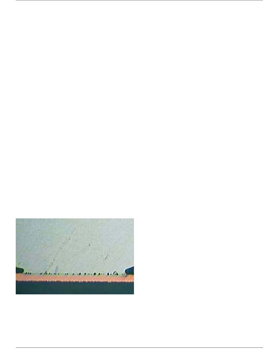
cern is micro voids or champagne voids that appear at the
ball to land interface (Figure 5-11); however, this problem
appears to have been mitigated with newer immersion sil-
ver chemistries.
5.3.3.6 Immersion Tin The immersion tin process uti-
lizes a displacement reaction between the copper surface
and tin ions in solution to reduce a layer of tin onto the
copper surface of the PCB. An organic substance is depos-
ited as part of the process that reduces the oxidation that
would be expected with a pure tin surface. Immersion tin
is compatible with SMT, BGA and through-hole compo-
nents but it is not wire-bondable. The chemistry and pro-
cess may not be compatible with some solder masks.
Immersion tin PCBs have a shelf life of 6 months. Previ-
ously shelf life was very limited (less than 6 months); how-
ever, in recent years it has improved considerably (see IPC-
4554). Tin dissolves into the solder and becomes part of the
solder joint; it is almost undetectable in the final solder
joint. Since the tin dissolves during soldering, the solder
joins directly to the copper surface. Immersion tin is com-
patible with tin/lead and lead-free solders. It provides a flat
surface which reduces stencil printing and component
coplanarity issues. There is some concern about tin whis-
ker formation but, with proper plating controls, it should
not occur.
Immersion tin finishes typically can only withstand 3 heat-
ing cycles without affecting solderability. Complete hole
fill at wave soldering may be difficult to achieve due to
immersion tin degradation after multiple reflow cycles,
especially when no-clean flux is used. It is a good idea to
use a nitrogen atmosphere during reflow soldering to limit
the amount of degradation; this will reduce the risk of hole
fill problems during wave soldering. It is also a good idea
to have a nitrogen atmosphere over the solder pot during
wave soldering, if possible.
5.4 Solder Mask The solder mask is a polymer coating
which serves to mask all surfaces which are not to be sol-
dered. Unlike the laminate, which is a composite, solder
mask is commonly a homogeneous material. As the name
suggests, this solder mask is used to mask off the surface
of the board where solder is not required to prevent bridg-
ing between conductors. Because of process changes for
lead-free soldering, evaluating solder mask performance
takes on a whole new meaning.
In the past, not all boards required a solder mask because
the conductors and lands were spaced quite far apart. With
the advent of fine lines and spaces, the use of a solder mask
has become almost mandatory for boards that are going to
be wave soldered. On a full SMT board where no wave
soldering is required, tenting or plugging of via holes is
done to assist drawing a vacuum on some ICT testers. Also,
the application of solder mask to block or plug a via allows
closer spacing between a via and the adjacent conductor
lines.
5.4.1 Wet and Dry Film Solder Masks Dry film solder
mask is no longer supported by major PCB suppliers. Addi-
tionally there is an overall solder mask thickness issue that
does not allow solder mask dams smaller than 0.25 mm.
Therefore, dry film solder mask is not suited for BGAs and
other fine pitch components. Wet (screened) mask is still
available; however, it too is not suited for BGA designs
because of registration challenges.
Figure 5-11 Example of Micro Voids
IPC-7095C January 2013
46
Copyright IPC-Association Connecting Electronics Industries
Provided by IHS under license with IPC
Not for Resale
No reproduction or networking permitted without license from IHS
--`,,```,,,,````-`-`,,`,,`,`,,`---

5.4.2 Photoimageable Solder Masks Photoimageable
solder masks provide accurate registration, are easy to
apply, encapsulate the circuit lines totally, have excellent
durability, and are cheaper than dry film.
Photoimageable masks can be either screened on or applied
by a process called curtain-coating in which the board is
passed at high speed through a curtain or waterfall of sol-
der mask.
The photoimageable mask may contain solvent along with
photopolymer liquid. If the solvent is added in the mask,
the liquid mask is screened on, solvent is dried off in an
oven, and then the mask is exposed to UV light by off-
contact or on-contact methods. (If no solvents are used, the
liquid is 100% reactive to UV light.) The off-contact
method requires a collimated light system to minimize dif-
fraction and scatter in liquid. This makes the system very
expensive. The on-contact approach needs no collimated
UV light source, and the system is relatively cheaper.
5.4.3 Jettable Solder Mask A new solder mask applica-
tion technology is becoming available to allow application
of solder mask in very fine pitch components. This technol-
ogy uses digital inkjet printer to print solder mask layer on
PCB or other substrates. The solder mask material is
applied directly on the substrate using digital data and set
of inkjet print heads with a resolution of 750 DPI.
The solder mask layer is implemented using one step as
opposed to using a four step process with the traditional
way of applying the solder mask. The solder mask material
is a specially-developed jettable ink. The ink is a solvent-
less hybrid system which is both UV and thermal curable.
Some of the advantages of the jetting system is the ability
to print narrow surface mount dams between fine-pitch
lands and tight control of the solder mask thickness. A few
disadvantages are that an end user must qualify the ink and
the material at the moment is only available in green color.
5.4.4 Registration of Board to Panel Image for Solder
Mask
Registration between individual boards within a
multi board panel becomes critical for any surface mount
application. This is especially true when the board is made
in a pallet format to assist the assembly process and
through-put characteristics. Board manufacturers inherently
build printed boards in a manufacturing panel format;
assemblers also want to take advantage of the multiple
board array format when they complete their assembly.
The positioning and orientation of individual boards on any
panel is usually at the discretion of the board manufacturer.
The manufacturer optimizes the use of the material in the
panel and the tolerance conditions that can be achieved
with the material used to build a particular board. It is a
well known fact that organic materials are prone to move-
ment (i.e. growth and/or shrinkage); thus, the board manu-
facturer, based on their knowledge of materials and their
predicted dimensional change movement, will commonly
adjust the photo tool of the circuit definition and the solder
mask definition to compensate for material stretch or
shrinkage depending on the circuit, the board size and the
particular properties of the selected solder mask material.
It is important to understand that assembly companies fre-
quently build their stencils based on a process of ‘‘step-
and-repeat’’ where elements of an individual board are
repeated to match the arrangement of the boards on the
subpanel. It is vital that the exact layout used by the board
manufacturer is understood to accurately provide the rela-
tionships of a land pattern for a BGA on one board with all
other land patterns of sister boards in the same panel.
Inconsistent arrangement of the assembly array can result
in misprints when stenciling solder paste onto the panel for
surface mount assembly.
5.4.5 Via Protection
5.4.5.1 Encroached vias
The encroached via concept is
one that permits solder mask being on the land without
filling the via plated-through hole. Encroachment vias take
the primary solder mask opening and adjust it so that it is
slightly larger than the via hole size.
This concept will permit any outgassing or cleaning of the
via plated-through hole, provide more surface coverage,
and increase adhesion between the solder mask and copper
of the annular ring. It will also provide a larger web
between the land and the via, and thus, should minimize
solder mask removal during BGA removal for rework.
5.4.5.2 Via Tenting, Plugging and Filling Via tenting,
plugging and filling (conductive or nonconductive) are
techniques used to cover or fill via holes with solder mask.
These processes serve different purposes. Via tenting, plug-
ging or filling is normally performed on boards that use
both reflow soldering and wave soldering. Via tenting,
plugging or filling is also recommended under certain
specified conditions, such as for boards where exposed vias
under BGAs are exposed to a wave solder. The concern is
based on the fact that, when a board with BGAs on the first
side is processed through wave soldering, a large amount
of heat can transfer from the vias. This can be very signifi-
cant because BGAs can have very high via densities
beneath them. The BGA’s joints can potentially reflow
again in the wave and a second reflow without flux could
result in cold solder joints or open joint conditions.
Via flooding and capping processing may be performed
after a surface finish has been applied. For OSP and ImAg
(immersion silver) finishes, via capping may be done after
the surface finish is applied because the harsh chemicals
that are used to clean the copper surface can become
trapped around the via cap. These trapped chemicals can
January 2013 IPC-7095C
47
Copyright IPC-Association Connecting Electronics Industries
Provided by IHS under license with IPC
Not for Resale
No reproduction or networking permitted without license from IHS
--`,,```,,,,````-`-`,,`,,`,`,,`---