IPC-7095C-2013.pdf - 第125页
is called Liquidus T ime Delay (L TD), and plays a critical role in HoP (see Figure 7-52). Looking at Figure 7-52, there are two T ALs. However , the T AL after collapse shown in the shaded area is the mini- mum required…
7.8.5 Head-on-Pillow BGA head-on-pillow (HoP) solder
joint is defined as a joint that is comprised of two metallur-
gical distinct masses. One formed from the BGA ball and
the other from the reflowed solder paste. They have incom-
plete or no coalescence. This defect is known by many
other names such as head and pillow, head in pillow, ball
in cup, ball in socket, and hidden pillow (see Figure 7-49).
The sequence of Head-on-Pillow defect formation is
explained in Figure 7-50. First, the BGA ball is placed on
the solder paste which has been printed on the printed cir-
cuit board (PCB) lands (Figure 7-50 (a)). As the BGA on
the PCB enters the reflow soldering oven and its tempera-
ture increases, a gap develops between the ball and the sol-
der paste due to some factor, such as dynamic warpage of
the package and/or PCB (Figure 7-50 (b)). The solder on
the PCB land melts and flux covers its surface. The solder
ball also melts and its surface, which typically has little or
no flux covering it, starts to oxidize (Figure 7-50 (c)),
When the BGA package collapses, the ball once again
makes contact with the molten solder paste mass. At this
time, if the ball and the molten solder paste mass coalesce
together, then a good solder joint is formed. But, if there is
insufficient flux activity and too much oxide coating on the
surface of the ball, it results in head-on-pillow.
7.8.5.1 Dynamic Warpage If the package warps during
reflow due to Coefficient of Thermal Expansion (CTE)
mismatch between the substrate and silicon as the package
temperature rises in the oven, the warping effect will cause
some solder balls to be lifted up from the solder paste on
the board. This action increases the oxide growth on the
surface of the ball as flux is left behind on the pad, leaving
the ball devoid of flux. Usually when package warpage is a
primary cause, the HoP defect will occur at the highest
warpage area of the package and adjacent joints will be
elongated. Figure 7-51 shows a high warpage BGA were
the corners are lifted resulting in HoP.
Boards may warp or sag during reflow resulting in
increased gap between the paste and the balls on the pack-
age. When the board is too thin and not supported during
reflow, board warpage can be a primary cause for HoP.
Usually when either board or package warpage is a primary
cause, more than one ball will show sign of HoP defect.
Also the adjacent joints will be elongated.
7.8.5.2 Reflow profile The reflow profile parameters
have strong impact on HoP because of temperature differ-
ential (dT). The dT can be seen within a single component
due to board design (copper distribution), laminate or pack-
age material, and the type and size of the package. There is
also dT between the outer and inner rows of BGA balls
because of airflow.
Generally, the temperature of the outer row of BGA balls
are higher than the temperature of inner row balls, result-
ing in time delay between outer and inner row balls melt-
ing. However, even though they melt at different times, the
package collapses only after the inner ball melt. This time
delay also exposes the outer two balls to high temperatures
for longer time without the protection of flux. This results
in their oxidation and, hence, contributes to HoP. This time
difference between inner and outer ball becoming liquidus
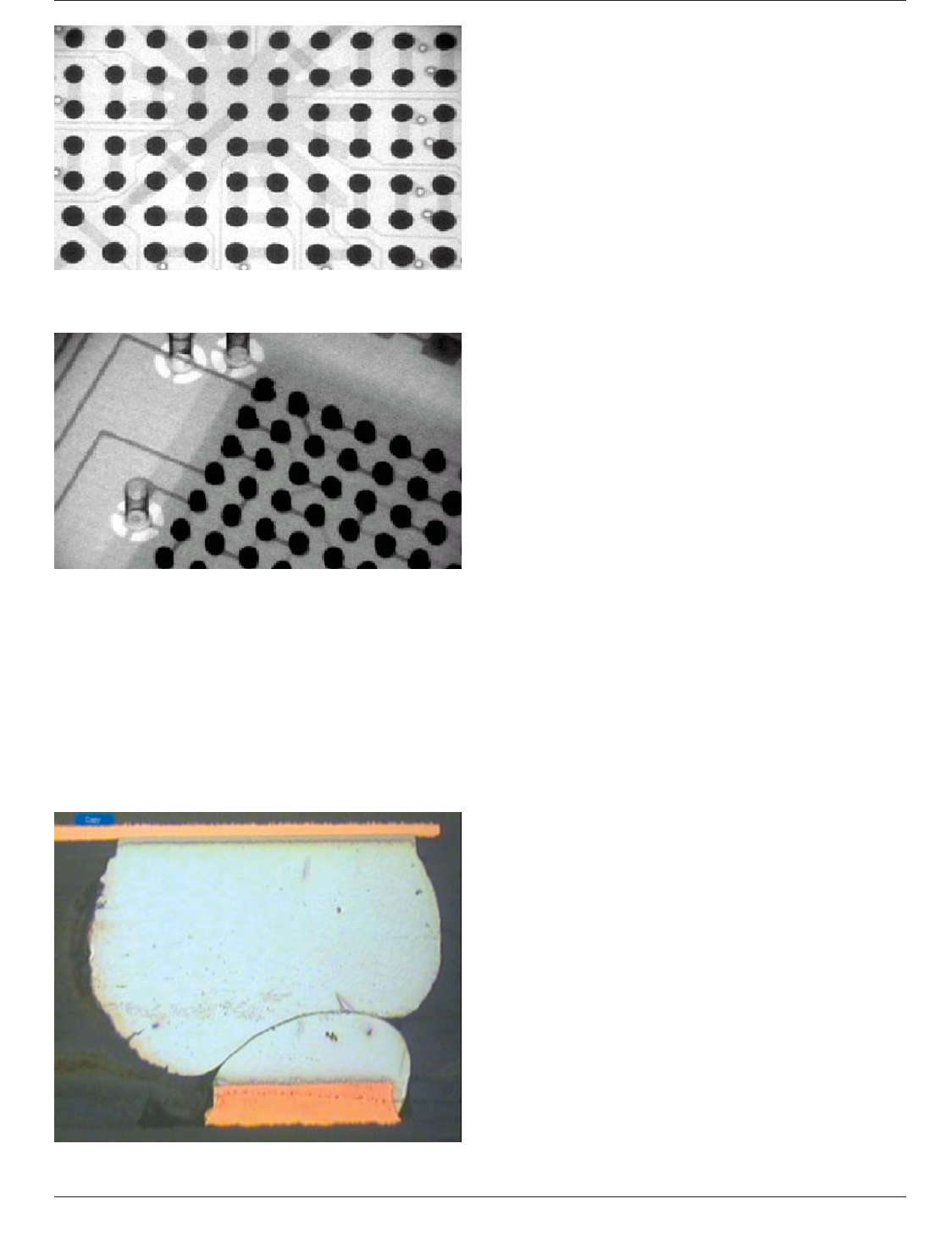
Figure 7-47 X-Ray Image Showing Uneven Heating
Note the solder balls are larger at the bottom than the top.
Figure 7-48 X-Ray Image at 45° Showing Insufficient Heat-
ing in One Corner of the BGA
Note the irregular shape of the solder bonds at the top of the image.
Figure 7-49 Example of Head-on-Pillow Showing Ball and
Solder Paste have not Coalesced
IPC-7095C January 2013
110
Copyright IPC-Association Connecting Electronics Industries
Provided by IHS under license with IPC
Not for Resale
No reproduction or networking permitted without license from IHS
--`,,```,,,,````-`-`,,`,,`,`,,`---
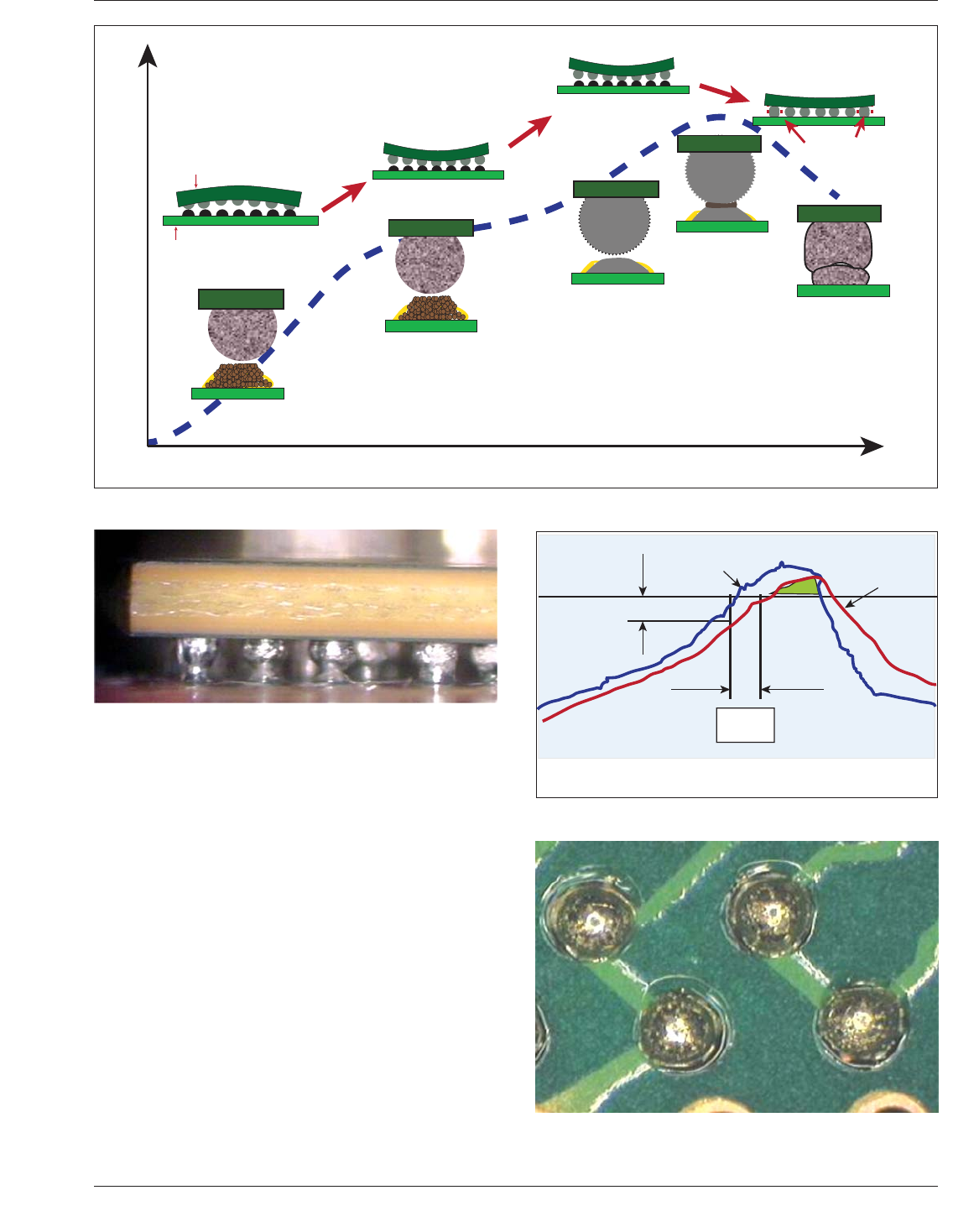
is called Liquidus Time Delay (LTD), and plays a critical
role in HoP (see Figure 7-52).
Looking at Figure 7-52, there are two TALs. However, the
TAL after collapse shown in the shaded area is the mini-
mum required TAL to achieve a good joint. In other words,
in order to minimize HoP, one must make sure that the true
TAL is long enough to form good joints.
7.8.5.3 Solder Paste The solder paste properties are
important to accommodate the soldering challenges of sol-
der ball excessive oxidation due to exposure to lead free
high temperatures and separation of the BGA ball from the
paste. Flux chemistry of these lead-free solders must have
adequate properties to prevent exhaustion of flux activation
in high temperature. Three key paste properties which
affect the HoP defect are: solder paste stability with time
and temperature, solder paste wettability, and the oxidation
resistance of the solder paste. Low oxidation resistant paste
implies that flux is not able to protect the solder powder’s
surface. There is high oxidation at outer surface also called
graping. Figure 7-53 shows paste printed on a board after
IPC-7095c-7-50
Figure 7-50 Head-on-Pillow Process Sequence Occurrences
Time
After BGA
placement
component
PCB
In Soak Zone
Above Solder
Melting Point
Head & Pillow
Defects
(a)
(b)
(c)
(d)
(e)
Temperature
Figure 7-51 HoP Due to High Package Warpage
Figure 7-52 Example of Liquidus Time Delay
220 ºC
Time [sec]
dT
Outer ball
Inner ball
LTD
Figure 7-53 Solder Particles on Board Noncoalesced After
Reflow
January 2013 IPC-7095C
111
Copyright IPC-Association Connecting Electronics Industries
Provided by IHS under license with IPC
Not for Resale
No reproduction or networking permitted without license from IHS
--`,,```,,,,````-`-`,,`,,`,`,,`---
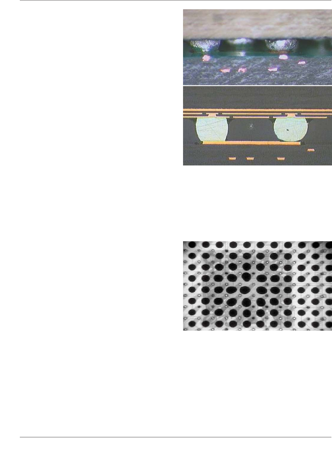
reflow. Non-coalesce of solder particles are seen, which
indicates that solder paste does not have good oxidation
resistance in the conditions it was reflowed.
7.8.5.4 How to Mitigate HoP Problem HoP is not an
easy defect to solve since there are many failure modes that
can cause this defect. In many cases, the HoP problem
consists of more than one failure mode at a time. The best
problem-solving approach would be to identify which are
the primary failure modes that need to be addressed to
eliminate HoP.
When a HoP problem exists, increasing solder paste vol-
ume will decrease the incidence of HoP. It may require
overprinting solder paste on some or all lands.
Some of the reflow parameters that have impact on HoP are
peak temperature and TAL. When dealing with HoP
defects, increasing TAL and peak temperature can decrease
the defect level by adding more time for the package to
contact the paste after full collapse and coalesce. One other
reflow parameter that could have an impact on HoP is soak
time. The impact depends on the type of paste used and its
behavior in high temperature. Follow the paste manufac-
ture recommendations and be sure not to stress and dry the
flux before reflow.
Using nitrogen in the reflow oven has been used to reduce
oxidation and increase SMT yield for HoP.
7.8.6 Hanging Ball/Non-Wet Open (NWO) A common
failure signature that is similar to head on pillow is head
with no pillow, which is known as nonwet open or hanging
ball. Failure happens in packages with high warpage. The
solder paste on the land adheres to the ball instead of
remaining on the land where it is supposed to be during
reflow. Because of package warpage, a gap is formed
between the package ball and the solder paste and the sol-
der sticks to the ball and coalesces with the ball. Oxide
builds up on the PCB land since it is exposed to high tem-
perature of reflow without the protection of flux resulting
in open joint known as hanging ball. Usually there is no
IMC formed on the land and it has the appearance of never
having any printed paste on it (see Figure 7-54).
Various factors affect hanging ball defects. They are type of
paste and flux, board land surface finish (OSP), land design
(SMD vs. MD) and copper on inner layers (thermal/ground
planes). To reduce occurrence of hanging balls, one should
change to a different solder paste chemistry, or add more
paste volume, or use nitrogen; all the solutions common to
HoP. Increasing the BGA land size also reduces hanging
ball incidence since a larger paste area provides more sur-
face tension and holds on to the paste instead of letting the
balls take the paste with them.
7.8.7 Component Defects Component defects such as
popcorning and warpage are generally caused by improper
handling of the BGA component prior to reflow. Both of
these problems produce a characteristic signature in the
X-ray image. Popcorning causes the BGA package to
expand below the die; resulting in an increase in size (and
possibly bridging) of the solder balls in the center of the
package as they are squished between the package and the
board (see Figure 7-55).
BGA warpage is more subtle than popcorning and can be
more difficult to detect in an X-ray image (see Figure
7-56). Warpage tends to be the largest at the corners of the
package. The X-ray image of a warped BGA tends to have
large elongated solder connections at the corner of the
package where warpage has occurred. The illustration in
Figure 7-56a shows the X-ray image and Figure 7-56b
shows a video microscope image of the package. Note that
in Figure 7-56b the ripple in the substrate, which is char-
acteristic of a stress relief which likely occurred during
reflow.
Figure 7-54 Hanging Ball Examples
Figure 7-55 X-Ray Image of Popcorning
IPC-7095C January 2013
112
Copyright IPC-Association Connecting Electronics Industries
Provided by IHS under license with IPC
Not for Resale
No reproduction or networking permitted without license from IHS
--`,,```,,,,````-`-`,,`,,`,`,,`---