IPC-7095C-2013.pdf - 第143页
factors that control stand-of f are land size, available solder volume, and the weight of the component. The lower the weight, the smaller the land size; the larger the solder vol- ume, the higher the stand-of f. 8.5.3 P…
coefficient of thermal expansion (CTE) for materials can
generate undue stress to the solder interface. The solder
attachment integrity for area array packages will vary,
depending on the loading conditions to which the solder
joints are subjected and the reliability requirements for the
product. CTE mismatch is further aggravated when large
silicon die are attached to an organic substrate with a non-
compliant epoxy compound. Silicon CTE is near 3 ppm/°C
while the organic substrate is closer to 16 ppm/°C. Package
warp during assembly processing and even the power dis-
sipation within the package can subject the solder joints to
significant tensile stresses. Excessive stress and strain at
the solder interface will cause solder joint failure and even
separation of the metallized lands.
When the die is attached to the package substrate with rigid
epoxy, the substrate material directly beneath the die may
be restricted to a CTE nearer that of the die. When solder
balls are retained in the same zone and exposed to a wide
variable of operating temperature, the solder interface will
be subjected to excessive strain. For ‘‘cavity-up’’ compo-
nents (die attached facing away from the package sub-
strate), only a thin dielectric layer separates the solder
joints from the die. The larger the die is, the more acute the
concerns for solder attachment reliability. Furthermore,
when the BGA solder joints fracture, they are typically near
the ball-to-package interface. This is a consequence of the
local expansion mismatch between the solder and the die-
constrained BGA substrate.
The current trend for larger BGA package outlines is to
move the contacts toward the package perimeter, with the
possible exception of some thermal solder balls and vias
retained at the central area of the package. Several manu-
facturers that cannot move the ball contact outside the die
attach area have adapted a more compliant die attach mate-
rial. The compliant die-to-package interface is slightly
thicker and exhibits a dramatic reduction in stress at the
solder-to-board interface, furnishing a substantial increase
in fatigue life.
8.5.2 Stand-Off Height Stand-off height significantly
affects reliability of solder joints. The higher the stand-off,
the better is the reliability of solder joints. BGAs attached
with Sn63Pb37 solder balls result in solder joint heights
that are less controlled and lower (height400 to 640 µm),
while the Sn10Pb90 solder balls (diameters of 760-890 µm)
result in uniform solder joint heights of the same dimen-
sion since the Sn10Pb90 solder has a Liquidus temperature
significantly above the near-eutectic tin/lead solders and
does not melt during a typical reflow process. Table 8-2
provides information on typical stand-off heights for tin/
lead ball and solder paste metallurgy packages.
Weight of the package also affects reliability of solder joint
since it impacts solder joint or stand-off height. The key
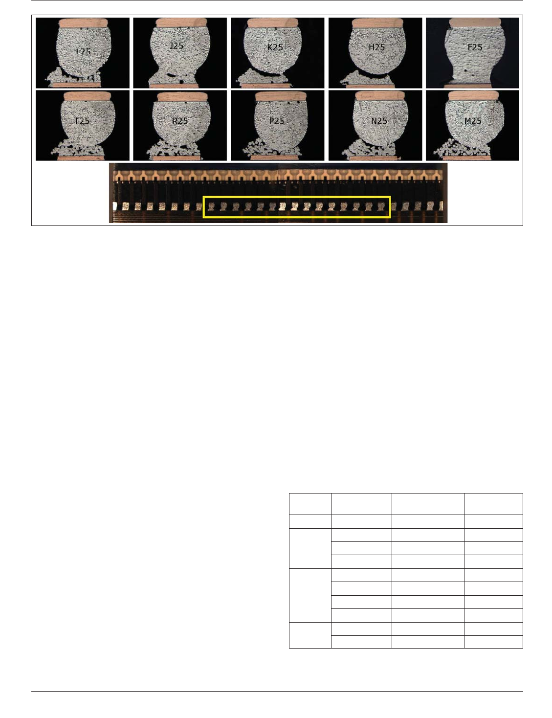
Figure 8-18 Cross-Section Photographs Illustrating Insufficient Melting of Solder Joints During Reflow Soldering. These
Solder Joints are Located Below the Cam of a Socket.
Table 8-2 Typical Stand-Off
Heights for Tin/Lead Balls (in mm)
Ball
Pitches
Stand-off
Heights
Ball Diameter
Prior to Reflow
PCB
Land Size
1.27 0.40-0.60 0.75 0.65
1.00
0.45-0.55 0.60 0.45
0.35-0.45 0.50 0.40
0.30-0.40 0.45 0.35
0.80
0.35-0.45 0.50 0.40
0.30-0.40 0.45 0.35
0.28-0.35 0.40 0.35
0.18-0.25 0.30 0.25
0.50
0.18-0.26 0.25 0.25
0.08-0.15 0.17 0.25
IPC-7095C January 2013
128
Copyright IPC-Association Connecting Electronics Industries
Provided by IHS under license with IPC
Not for Resale
No reproduction or networking permitted without license from IHS
--`,,```,,,,````-`-`,,`,,`,`,,`---
factors that control stand-off are land size, available solder
volume, and the weight of the component. The lower the
weight, the smaller the land size; the larger the solder vol-
ume, the higher the stand-off.
8.5.3 PCB Design Considerations Another influence on
reliability is the geometry of the solder joints as well as the
solder land metallization. Solder masks can have a negative
influence if they are used for solder mask-defined (SMD)
lands with the solder mask on the metallization lands
affecting the solder joint geometries. Stress concentrations
created by the SMD solder joint geometries can be the ori-
gin of solder joint failures and reduced reliability. More
than that, the solder mask shape and thickness could influ-
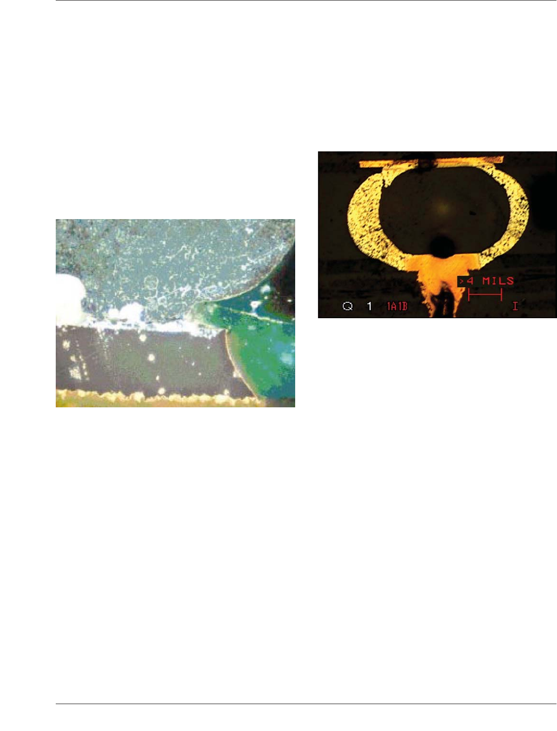
ence the reliability of the solder joint. Figure 8-19 shows
crack due to stress concentration at the solder mask.
For equal solder joint height, increases in fatigue life by
factors of about 1.25 to 3 can be anticipated with the use
of nonsoldermask-defined (NSMD) vs. SMD lands with the
larger improvements for solder joints with the more severe
loading conditions. Surface finish also plays a critical role
in BGA solder joint reliability. HASL, a commonly used
surface finish may be too thick or too thin. Insufficient sol-
der thickness may be consumed as intermetallic, which is
unsolderable. Immersion gold over electroless nickel is
prone to the black pad defect which leads to brittle interfa-
cial solder joint failures under mechanical and/or thermal
stress. The ‘‘black pad’’ defect is thought to be caused by
excessive corrosion of the nickel during the gold plating
process.
Laminate cracking is also a possible failure mechanism
under BGA solder joint lands. Such failure is thought to be
caused by thermal mechanical stress during reflow and or
subsequent mechanical stresses on the joints. Via-in-pad or
via next to land may cause drainage of solder. This is gen-
erally not recommended. Via-in-pad is being tried by some
companies with successful results. However, such an
approach should be considered only by companies with
extensive internal resources to validate reliability of solder
joints with via in pad technology.
Microvias are becoming more common in BGA lands.
Most of the BGAs will have voids whenever microvias are
used. Studies showed that most voids are not a reliability
risk to initiate a crack, however, they reduce the joint area
and will shorten the time to failure when a crack is propa-
gated. Figure 8-20 shows a failure after reliability testing
where the void was so large the ball collapsed.
8.5.4 Reliability of Solder Attachments of Ceramic Grid
Array
Ceramic CTE is about 6 ppm/°C; the CTE of
organic-based PCBs is in the range of 16-20 ppm/°C. Thus,
a global CTE-mismatch of about 10-14 ppm/°C exists
between ceramic components and organic printed boards.
To compensate for the large global CTE-mismatch, ceramic
components typically require solder columns to function
reliably in most applications. Since the corner joints are
loaded more than other solder joints (they are farthest from
the neutral point or DNP), they fail first.
The solder columns, which currently are only used for
ceramic Grid Array Components (GACs), are 10Sn/90Pb
columns with lengths of 1.27 mm to 2.29 mm that are
either cast onto the CGA or are wire soldered to both the
CGA and the substrate with near-eutectic tin/lead solder.
With all other conditions being equal, the ratio of CBGA
solder joint fatigue lives of three column heights, 0.41 mm
[16 mils], 0.76 mm [30 mils], 2.29 mm [90 mils] is 1:4:45.
The height of the solder columns is limited by the require-
ment that the column aspect ratio (height-to-diameter) does
not produce slender columns thus changing the loading
conditions; cast columns can accommodate larger aspect
ratios.
8.5.5 Lead-Free Soldering of BGAs This section covers
various aspects of board assembly of BGAs using lead-free
solders. A description of various available lead-free alloys
and their selection is described first. Board design and
Figure 8-19 Solder Mask Influence
Figure 8-20 Reliability Test Failure Due to Very Large Void
January 2013 IPC-7095C
129
Copyright IPC-Association Connecting Electronics Industries
Provided by IHS under license with IPC
Not for Resale
No reproduction or networking permitted without license from IHS
--`,,```,,,,````-`-`,,`,,`,`,,`---

assembly consideration for BGAs are described next with
a discussion on the transition technologies that occur when
converting from a tin/lead to a lead-free package and
assembly concluding this section.
8.5.5.1 Lead-Free Alloy Selection Ideally, the lead-free
alloys selected should be drop-in replacements for the cur-
rently used tin/lead (Sn-Pb) alloys. Drop-in replacement
alloys do not require any significant change in the materi-
als, equipment and processes for package and board assem-
bly. Drop-in replacement does exist, but the cost of these
drop-in replacements are not on parity with that of alloys
that require higher process temperatures (e.g., SAC305)
within the list of potential lead-free solder alloys that are
currently available.
The seminal work to select the best lead-free solder alloys
in existence was the three year study undertaken by the
National Center for Manufacturing Sciences (NCMS). This
study culminated in a report that covered the evaluation of
over 79 lead-free solder alloys.
Table 8-3 shows some of the common lead-free solders that
were evaluated by the NCMS group. These are listed
according to their melting points. The overwhelming
majority of these alloys are tin-rich alloys (>90%Sn) with
Sn respectively forming binary or ternary systems with
other elements such as Bi, Zn, Sb, Ag, and Cu. The melt-
ing points and the advantages and drawbacks for these
alloy systems as well as other potential alternatives are
listed in the table.
The binary and ternary tin-rich alloys, except the Sn-Zn
system, noticeably have 30-40°C higher melting points
than eutectic tin/lead solder (melting point, mp = 183°C).
Alloys with comparable melting points while possessing
the desirable physical and mechanical properties, suitable
for SMT assembly have to extend to quarternary alloys.
Some consortia around the world have selected alloys from
the Sn-Ag-Cu family as the lead-free solders of choice. In
determining this final choice of the alloy family as well as
the particular alloy compositions, many factors were con-
sidered and evaluated. These included:
• Melting temperature
• Wettability to common component substrate and board
surface finishes
• Compatibility to common fluxes, particularly no-clean
fluxes
• Component and board reliability
Table 8-3 Common Solders, Their Melting Points, Advantages and Drawbacks
Alloys or Alloy
Systems
Melting
Point (°C) Advantages Drawbacks
Sn95Sb5 240 Good fatigue resistance.
Higher toxicity than lead; high melting
temperature; 8°C pasty range; poor wetting;
low tensile strength.
Sn99.3Cu0.7 227
Low cost in comparison to other lead-free
solders; not prone to fillet lifting in the absence
of lead.
Reduced wettability in air, but adequate in an
inert atmosphere.
Sn96.5Ag3.5 221
One of the primary choices by NCMS study;
used for many years in certain applications;
fatigue properties are similar to tin/lead solders
for some accelerated reliability
test results.
Poorest wetting in reflow soldering among
high-tin alloys; though wettability still adequate
for most board assembly operations.
SnAgCu 217-220
Better creep resistance than tin/lead solders;
fatigue properties are better than tin/lead
solders for some accelerated reliability test
results. Optimum pasty range for tombstone
control.
Prone to fracture in high shock applications.
Some compositions are patented.
SnZnBi 191-199
Closest in melting point to tin/lead alloys;
better strength than tin/lead solders; fatigue
properties are better than tin/lead solders for
some accelerated reliability test results.
Very susceptible to oxidation and corrosion
but small amount of Al could alleviate these
problems; requires special fluxes and solder
processes for achieving acceptable manu-
facturing yields.
Sn91Zn9 199
Sn63Pb37 183 Most widely used solder alloy. Contains lead.
Sn62Pb36Ag2 179
Higher tensile strength, pasty range for
anti-tombstone, greater creep resistance
Contains lead, more expensive.
Bi58Sn42 139
One of the alloys down-selected by NCMS;
presently used in low temperature applications.
Melting point is too low for computer
applications; susceptible to formation of low
melting ternary phase by lead contamination.
In52Sn48 118 One of the lowest melting point solders.
Indium supplies are limited; melting point too
low for computer applications; susceptible to
corrosion.
IPC-7095C January 2013
130
Copyright IPC-Association Connecting Electronics Industries
Provided by IHS under license with IPC
Not for Resale
No reproduction or networking permitted without license from IHS
--`,,```,,,,````-`-`,,`,,`,`,,`---