IPC-7095C-2013.pdf - 第25页
thus such terms as ‘ ‘frowning’ ’ or ‘ ‘smiling’ ’ BGAs have been used to identify these conditions. The so-called ‘ ‘smil- ing’ ’ BGA interposer puts a stress on the balls at the outer rows, while the ‘ ‘frowning’ ’ BGA…

BGA issues are not insurmountable; however, they require
dedicated engineering resources to develop and implement
a consistently reliable process.
3.5.1 Visual Inspection BGA is not a package suitable
for companies that assure quality by inspection and repair.
BGA solder joints cannot be inspected unless X-ray or
optical inspection techniques are used. To reap the benefits
that BGA offers, robust process control must be main-
tained. Due to limited time and training, many companies
find implementing such tight process control to be a diffi-
cult endeavor.
There are some visual inspections of BGAs that can iden-
tify problems with solder joints. These would show good
flow on an uncollapsed ball with ceramic BGAs, and also
be able to show collapsed balls on plastic BGAs on the
outer rows of the BGA. Visual inspection of the outer rows
serves as an indicator of some of these problems. Examples
are BGA alignment with the lands on the outer rows, and
how the BGA is sitting on the board, level or skewed.
3.5.2 Moisture Sensitivity The plastic BGA packages
are very moisture sensitive. This makes them susceptible to
warpage, swelling, popcorning, or cracking if the packages
are not properly baked and kept dry prior to package
assembly. Component storage and handling procedures are
critical for any moisture sensitive component including
leaded surface mounted devices, but it is critical for BGAs/
FBGAs.
Component moisture sensitivity is tested using J-STD-020
and is determined according to the package thickness. The
moisture sensitivity level must be analyzed for each BGA
package type. It is critical to know at which of the appli-
cable temperatures, 220°C, 235°C, 245°C, 250°C, or
260°C the BGA package was classified. The classification
of the package type may drop several levels if the higher
temperature is used.
Due to improvements in molding compounds and laminate
systems, most laminate-based BGAs can be mounted and
qualified for temperatures above 220°C. The hermetic
ceramic BGAs are not moisture sensitive and therefore can
be mounted using either of the higher temperatures.
Because of the switch to lead-free solders, the industry
needs to test and verify at a higher temperature such as
260°C, which will create major issues with not only BGAs,
but also all surface mounted devices.
3.5.3 Thermally Unbalanced BGA Design The plastic
BGA package is also susceptible to warpage at which time
the package edges lift up; this could result in no connec-
tions on the outer rows. The edges may also bend down,
Table 3-3 Potential Plating or Component Termination Material Properties
Gold (Au)
Gold (Au), electroplated
Gold (Au), hard
Indium (In)
Nickel/Gold (Ni/Au) ENIG
Nickel/Gold (Ni/Au), electrolytic
Nickel/Gold (Ni/Au),
Nickel/Palladium (Ni/Pd)
Nickel/Palladium/Gold (Ni/Pd/Au)
Nickel/Palladium/Gold (Ni/Pd/Au), ENEPIG
Organic Solderability Preservative (OSP)
Organic Solderability Preservative (OSP-HT), high temp
Palladium (Pd)
Platinum/Palladium/Silver (Pt/Pd/Ag)
Silver (Ag)
Silver (Ag), electroplated
Silver (Ag), immersion
Silver (Ag), with Nickel (Ni) barrier
Silver/Palladium (Ag/Pd))
Silver/Palladium (Ag/Pd), with Nickel (Ni) barrier
Tin (Sn)
Tin (Sn), bright
Tin (Sn), bright, annealed
Tin (Sn), bright, fused
Tin (Sn), bright, reflowed
Tin (Sn), bright, reflowed over Nickel (Ni) barrier
Tin (Sn), bright, with Nickel (Ni) barrier
Tin (Sn), bright, with Silver (Ag) barrier
Tin (Sn), hot dipped
Tin (Sn), immersion
Tin (Sn), matte
Tin (Sn), matte, annealed
Tin (Sn), matte, fused
Tin (Sn), matte, reflowed
Tin (Sn), matte, reflowed over Nickel (Ni) barrier
Tin (Sn), matte, with Nickel (Ni) barrier
Tin (Sn), matte, with Silver (Ag) barrier
Tin (Sn), reflowed
Tin (Sn), Semi-matte (Sn)
Tin/Bismuth (SnBi), <5% Bi
Tin/Bismuth (SnBi), =>5% Bi
Tin/Bismuth/Gold (Sn/Bi/Au)
Tin/Copper (Sn/Cu)
Tin/Copper (Sn/Cu), annealed
Tin/Copper (Sn/Cu), HASL
Tin/Copper (Sn/Cu), hot dipped
Tin/Copper (Sn/Cu) matte
Tin/Lead (Sn63Pb37)
Tin/Lead (Sn90Pb05)
Tin/Lead/Silver (Sn/Pb/Ag)
Tin/Silver (Sn/Ag)
Tin/Silver (Sn/Ag), hot dipped
Tin/Silver (Sn/Ag), plated
Tin/Silver/Bismuth (Sn/Ag/Bi)
Tin/Silver/Bismuth/Copper (Sn/Ag/Bi/Cu)
Tin/Silver/Copper (Sn/Ag/Cu)
Tin/Silver/Copper (Sn/Ag/Cu), hot dipped
Tin/Zinc (Sn/Zn)
Tin/Zinc/Aluminum (Sn/Zn/Al)
Tin/Zinc/Nickel (Sn/Zn/Ni)
NAC* (Not applicable - Must provide Comment)
IPC-7095C January 2013
10
Copyright IPC-Association Connecting Electronics Industries
Provided by IHS under license with IPC
Not for Resale
No reproduction or networking permitted without license from IHS
--`,,```,,,,````-`-`,,`,,`,`,,`---
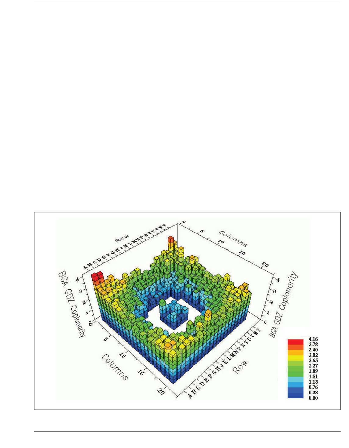
thus such terms as ‘‘frowning’’ or ‘‘smiling’’ BGAs have
been used to identify these conditions. The so-called ‘‘smil-
ing’’ BGA interposer puts a stress on the balls at the outer
rows, while the ‘‘frowning’’ BGA interposer puts the stress
on the connection of the inner row ball locations. Package
warpage is of real concern in flux-only applications during
rework. Large die sizes can cause CTE mismatch between
the PCB and the package laminate material, which can cre-
ate package warpage (see Figure 3-8).
Thermally unbalanced package designs, particularly those
with heat spreaders on the top, will warp according to the
classic bi-metal effect.
3.5.4 Rework Although BGAs do not require nearly as
much rework as fine pitch lead-frame devices, many
assemblers are apprehensive about using a component
package that is difficult to be reworked. While BGA rework
is difficult, it is by no means impossible. Tools and tech-
niques for rework are currently available that range from
manual to automated techniques to reball the BGA or
redress the land pattern. Several factors must be addressed
during the rework operation. These are:
• Number of heat cycles
• Ball collapse during re-balling
• No damage to pads on BGA interposer
• Proper land redressing and no damage to lands on the
product board
• Appropriate reflow temperature for re-attachment based
on alloy used
• Proper cleaning to remove flux residue unless no-clean
flux is used
3.5.5 Cost The BGA still has a slight cost differential
compared to fine pitch peripheral packages that it replaces.
However, competitive pressures keep bringing costs lower
to meet new targets. Further costs accrue with the increased
board layer counts that BGAs require; however, there are
many advantages to the interconnecting concepts and the
performance characteristics resulting from BGA implemen-
tation.
Following are some of the key reasons for higher BGA
package cost:
• Higher cost substrate (fine line/space)
• High T
g
BT (bismaleimide-triazine) resin
• Thermal enhancements
• Electrical enhancements
• Very fine external pitches
• High temperature reflow requirements
• Thin profile heights
IPC-7095c-3-8
Figure 3-8 BGA Warpage
January 2013 IPC-7095C
11
Copyright IPC-Association Connecting Electronics Industries
Provided by IHS under license with IPC
Not for Resale
No reproduction or networking permitted without license from IHS
--`,,```,,,,````-`-`,,`,,`,`,,`---

All of these have been addressed in the last few years and
great progress has been made.
In general, it has been difficult to create standard pin count
BGA designs because every die has different requirements.
Each package/die combination is unique; therefore, econo-
mies of scale that manufacturers can achieve with
perimeter-leaded packages are not necessarily seen with the
area array devices.
Table 3-4 shows the expectations of the semiconductor
industry as to what they expect to pay on a cost per pin
relationship for the different technologies over the next
several years. The shaded sections indicate a challenge and
degree of difficulty in achieving the predicted goals. Table
3-4 is taken from the ITRS 2010 Roadmap and the costs
are very aggressive. The lower range of costs reflects
peripheral leaded packages and the higher ranges reflect
array style packages like BGAs/FBGAs.
The opinion of many resource experts is that the prices in
the future years may not be able to be achieved with prof-
itability because of the low costs forecasted.
3.5.6 Availability The 1.27 through 0.8 mm are available
in high volumes in many locations in the world. The
0.50 mm and below pitch packages are also becoming
available, and are used in many advanced portable elec-
tronic applications. Some of the component manufacturers
are developing their own version of the BGA package. Part
of this has to do with making it more difficult to copy the
design; another part has to do with maintaining market
share. The concept is one that prevents second source entry
and locks the designer that chooses a particular nonstan-
dard component product into a single component supplier.
3.5.7 Voids in BGA Many companies use X-ray,
In-circuit Test (ICT) and Automatic Optical Inspection
(AOI) in combination to improve their process control for
BGA solder joints. Some look for voids through X-ray to
determine accept/reject criteria. Some level of voiding in
any kind of solder joint is inevitable, but there is still
debate as to what is acceptable or an excessive void. The
proponents of voids argue that it is not the void that is bad,
but its location. The review of voiding has many consider-
ations, and in order to assist in process improvement
criteria, several tables in Appendix A are available to assist
in establishing process improvement goals. The informa-
tion on voiding has been analyzed in many controlled
experiments with no correlation being established that
relates the amount of voiding to reliability performance
under thermal or mechanical stress.
As the pitch of the BGAs become smaller and the ball size
is reduced, the number of voids in an individual ball
becomes more of a concern. One suggestion has been to
correlate void acceptance to the environment in which the
final product must perform. It is recommended that each
product establish a criterion for a Void Protocol which
would establish the goals for a process or a product.
3.5.8 Pad Cratering A new concern for BGA implemen-
tation is the phenomena of pad cratering. Pad cratering is
defined as a separation of the pad from the PCB resin/
weave composite or within the composite immediately
adjacent to the pad. It is also known as a ‘‘laminate crack.’’
Examples of pad cratering are shown in cross-section pic-
tures of BGA solder joints in Figure 3-9. Much of the rea-
son for this condition rests with the new formulations for
laminate resin systems that have been formulated to meet
the higher temperature requirements of the lead-free solder.
Some of the new materials are stiffer and may be more
brittle than those used in the past.
There are several possible failure modes for a BGA solder
joint. The different conditions are depicted in Figure 3-10
which is intended to highlight the location of pad cratering
in relation to other forms of solder joint failures. The Pad
Crater failure mode is in location 5. It occurs between the
land pad and the PCB laminate. The failure between the
component substrate and the component pad at location 1
is also very similar to pad cratering, but this type of failure
is usually attributed to the component packaging process
rather than the printed board assembly. The occurrence of
failure in location 1 is usually discovered during compo-
nent reliability evaluations or during the classification con-
ditioning described in paragraph 3.5.2.
3.5.9 Standardization Issues Many of the BGAs are
using conventional printed board (interposer) materials but
are being tested to the standard component reliability tests.
Table 3-4 Example of Semiconductor Cost Predictions
Year Roadmap Input 2008 2009 2010 2011 2012 2015 2018 2020
Cost per Pin Minimum for Contract Assembly [1,2] (Cents/Pin)
Low-cost, hand held and memory 0.24-0.47 0.23-0.46 0.22-0.45 0.21-0.43 0.20-0.42 0.19-0.38 0.18-0.35 0.17-0.34
Cost-Performance 0.63-1.00 0.62-0.96 0.61-0.94 0.60-0.92 0.58-0.90 0.55-0.85 0.52-0.80 0.50-0.79
High-Performance 1.68 1.64 1.61 1.58 1.55 1.45 1.37 1.32
Harsh 0.23-2.00 0.22-1.90 0.22-1.54 0.21-1.46 0.20-1.38 0.19-1.17 0.18-1.00 0.17-0.89
White - Solutions exist Yellow - Solutions being pursued Red - No known solutions
IPC-7095C January 2013
12
Copyright IPC-Association Connecting Electronics Industries
Provided by IHS under license with IPC
Not for Resale
No reproduction or networking permitted without license from IHS
--`,,```,,,,````-`-`,,`,,`,`,,`---