IPC-7095C-2013.pdf - 第66页
should be distinct enough so as not to be confused with any other markings around the land pattern. 6.2 Attachment Sites (Land Patterns and Vias) 6.2.1 Big vs. Small Land and Impact on Routing The diameter of the solder …
Nearly all hot air methods use a nozzle system that fits
down over and/or around the BGA package to heat the sol-
der joints for removal and reflow. A component keepout
area of 2.5 mm away from the outer edge of the oven
nozzle is suggested. Including the nozzle size results in a
3.8 mm clearance from the component body. This spacing
around the BGA provides room for the nozzle and reduces
the risk of heating solder joints of adjacent components
above the reflow temperature. When using laser for rework,
the keepout area can be reduced to under 1 mm.
After a BGA package has been removed from the board
during repair, the solder lands must be cleaned and new
solder paste or flux applied before a new component can be
placed. If the solder paste or flux is dispensed using manual
methods, or if solder paste is applied using an automated
dispensing system, then there are no special component
keepout areas required. However, many repair systems use
a miniaturized stencil and squeegee to manually apply sol-
der paste either to the lands on the board or onto the balls
of the component. In general, a minimum of 3 mm compo-
nent keepout (i.e., the nominal distance between the body
of the component and the body of the neighboring compo-
nent) is needed so that both the nozzle clearance require-
ment and the mini-stencil requirement can be met when
printing to the lands on the board. The existence of a high
profile neighboring component may require the minimum
distance to be much larger than the stated minimum value.
6.1.3 Global Placement There are no special global
placement requirements for BGA packages. However, it is
recommended that they not be placed near the board cen-
terlines. This reduces the potential of coplanarity problems
associated with the board warping during reflow. In addi-
tion, BGA packages should not be placed next to large
through-hole components, as these can stiffen the board
and significantly increase localized BGA corner joint
stresses. In some cases, one might want to take advantage
of certain features that might actually help protect the BGA
if the induced strain relative to the BGA corners are
reduced by the stiffness caused by nearby through-hole or
other components. Finally, BGA packages should not be
placed with their diagonals in line with mounting stand-off,
bosses, and screws that support or secure the printed board
assembly, since this can induce levels of stress on the cor-
ner balls, which are more susceptible to damage.
6.1.4 Alignment Legends (Silkscreen, Copper Features,
Pin 1 Identifier)
Alignment features printed on the circuit
board are recommended for BGA packages to verify com-
ponent alignment before and after reflow. BGA packages,
especially PBGA, will self-align during reflow, even when
placed up to 50% off the lands. As a result, any misalign-
ments are generally one land diameter length or more off.
Alignment features will help verify that the component
placement is sufficiently accurate with visual inspection.
Silkscreen and copper are the two main materials used for
alignment legends. Silkscreen is the most visible material,
but requires the additional process step during board manu-
facturing. Copper alignment legends are created at the
same time all other copper features are created and, there-
fore, lead to more accurate placement. Higher speed cir-
cuitry may be affected by the ungrounded copper in this
solution. Unconnected copper conductors can collect a
capacitance which will dissipate uncontrollably.
In many instances, legends are used by equipment or indi-
viduals to evaluate the alignment of the BGA during the
placement operation. For peripheral leaded components,
the fiducial has been standardized so that placement equip-
ment can adjust the movement of the placement head
accordingly and improve the final component positioning.
Local fiducials are often placed at opposite corners to allow
adjustment for the theta angle. This technique has been
incorporated into many placement tools and equipment.
The use of fiducials may not provide the most obvious
condition for human inspection; however, most inspectors
can approximate that the package is properly centered
between two fiducials in order to verify their position. In
some instances, companies have used angle brackets in
place of the fiducials to assist the human eye in making this
judgment; however, the camera for placement equipment is
not familiar with that configuration, thus the practice is not
the most conducive for automatic assembly (see Figure
6-1).
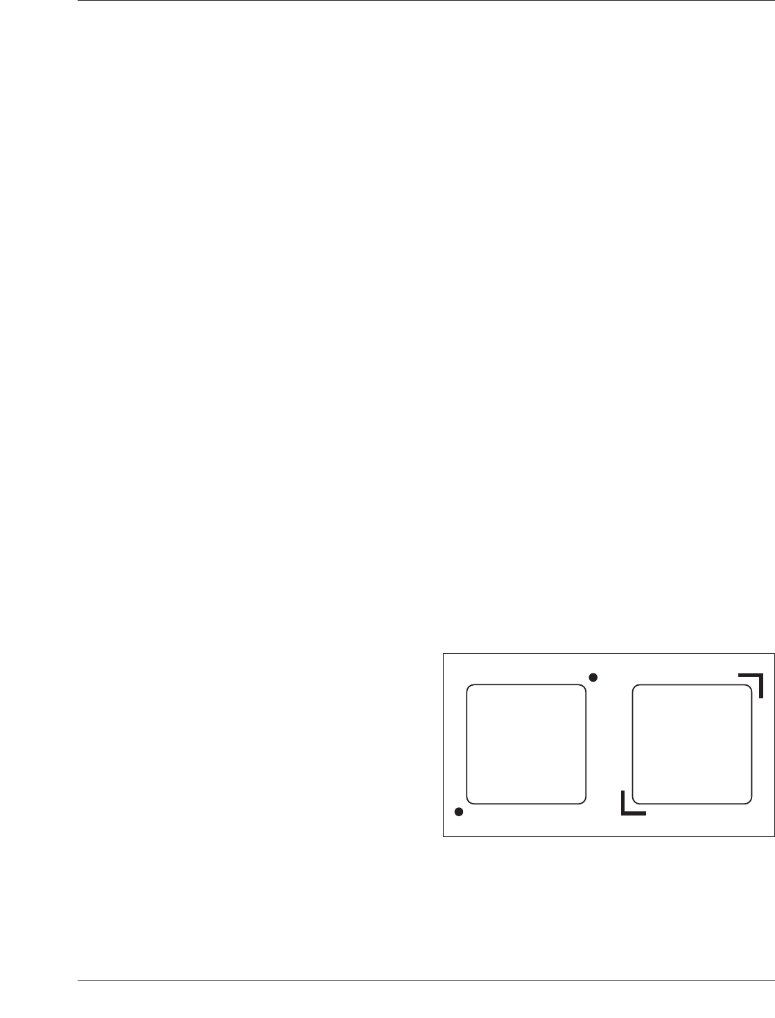
Using silkscreen, the entire package can be outlined for
easy visual alignment. Another alignment pattern com-
monly used is to mark just the corners of the BGA pack-
age. Corner marks should only be 0.8 mm long on each
side. Copper can be used for corner marks, since it won’t
interfere with routing runs, as long as it does not affect cir-
cuitry performance such as unwanted capacitance.
All alignment legends should be offset 0.25 mm away from
the outer edge of the BGA package. This gives sufficient
clearance to view the features all around the BGA package.
Pin 1 identifiers are required on BGA land patterns. This
identifier can be a caret, dot, or other easily visible shape.
The Pin 1 identifier can be either silkscreen or copper and
IPC-7095c-6-1
Figure 6-1 BGA Alignment Marks
January 2013 IPC-7095C
51
Copyright IPC-Association Connecting Electronics Industries
Provided by IHS under license with IPC
Not for Resale
No reproduction or networking permitted without license from IHS
--`,,```,,,,````-`-`,,`,,`,`,,`---
should be distinct enough so as not to be confused with any
other markings around the land pattern.
6.2 Attachment Sites (Land Patterns and Vias)
6.2.1 Big vs. Small Land and Impact on Routing
The
diameter of the solder land can affect both the reliability of
the solder joints and also the routing of conductors. The
land diameter is usually smaller than the ball diameter of
the BGA. The land size reduction of 20 to 25% has been
determined to provide reliable attachment criteria. The
larger the lands the less room for routing between lands.
For example, a 1.27 mm pitch BGA package with 0.63 mm
diameter solder lands will be able to fit two conductors
between the lands using 125/125 µm conductors and
spacing. If a 0.8 mm diameter solder land is used, only
one conductor can fit between the solder lands using 125/
125 µm conductors and spaces.
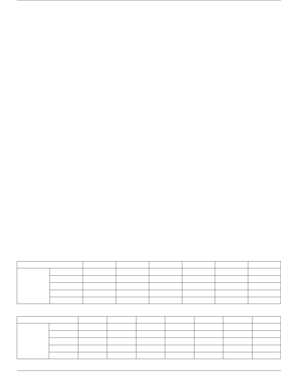
Tables 6-1 and 6-2 show the number of conductors that can
be routed between lands for various land diameters and
conductor/space widths.
The following equation can be used to determine the num-
ber of conductors that can be routed between lands depend-
ing on package pitch (P), solder land diameter (D), number
of conductors between lands (n) and conductor/space width
(x).
P-D≥ (2n + 1)x
A general rule is to design the solder land on the circuit
board with the same diameter as the solder land on the
plastic BGA substrate.
Table 6-3 shows another view that takes the maximum land
size possible for a particular number of conductors instead
of number of conductors for each land size and has addi-
tional pitches. Information is also provided on interstitial
via.
Solder land sizes for a CBGA should be designed such that
the noncollapsing ball or column has sufficient platform
availability of the land in order to obtain the solder attach-
ment to the column or ball of the CBGA. This makes the
land somewhat larger in order to establish this minimum
requirement and is necessary to ensure reliability of solder
joints which usually comes from the melted solder paste
deposit.
6.2.2 Solder Mask vs. Metal Defined Land Design
There are two basic types of solder lands used for BGA
packages. These are metal defined (MD) and solder mask
defined (SMD). MD lands are etch-defined and there is
solder mask clearance around the lands, similar to most
surface mount lands. SMD lands have solder mask overlap-
ping the copper land (see Figure 6-2). Both land types have
advantages and disadvantages.
6.2.2.1 Metal Defined Lands Metal-defined (MD) lands
require a smaller diameter copper land and, therefore, have
more metal-to-metal spacing for routing and vias. Copper
dimensions can also be controlled better than solder mask
dimensions, giving a more uniform surface finish, espe-
cially for HASL boards. The absence of solder mask
around the solder land allows the solder to flow around the
edges of the land, eliminating any areas of stress concen-
tration.
Metal defined lands give the solder joint a much better
geometry but result in a lower standoff height (see Figure
6-3). This improved geometry may potentially improve
fatigue resistance; however, the lower standoff height may
negate some of the improvement to fatigue resistance.
6.2.2.2 Solder Mask Defined (SMD) Lands Because of
the overlapped solder mask, SMD lands require a larger
diameter metal land to achieve the same sized land diam-
eter as MD. The solder joint is defined by the solder mask
creating a stress concentration (see Figure 6-4), but will
Table 6-1 Number of Conductors Between Solder Lands for 1.27 mm Pitch BGAs
Solder Land Diameter (micron) 750 700 625 500 400 350
Conductor
Spacing
Width (µm)
200N/AN/A1111
150111222
125112223
100222334
75233455
Table 6-2 Number of Conductors Between Solder Lands for 1.0 mm Pitch BGAs
Solder Land Diameter 625 500 400 350 300 250 200
Conductor
Spacing
Width (µm)
200N/AN/A11111
150N/A111122
1251112222
1001222233
752233444
IPC-7095C January 2013
52
Copyright IPC-Association Connecting Electronics Industries
Provided by IHS under license with IPC
Not for Resale
No reproduction or networking permitted without license from IHS
--`,,```,,,,````-`-`,,`,,`,`,,`---
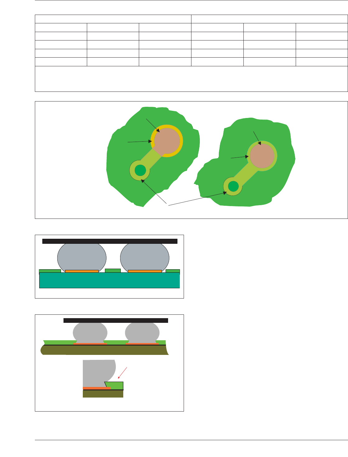
have a higher standoff. The effect is illustrated in Figure
6-5, which shows the contrast in joint geometry resulting
from solder mask defined lands (left side) and a metal
defined condition (right side). The stress concentration on
the solder mask defined land results in possible crack ini-
tiation at the mounting surface. The SMD lands adhere to
the board better because of the larger surface area of cop-
per and the overlapping solder mask. The major disadvan-
tage to SMD lands is the vulnerability of the solder joint at
the interface of solder mask and solder material. Some tests
indicate that the solder joint fatigue life has decreased sig-
nificantly when compared with nonsolder mask defined
(MD) lands. The major advantage is that this approach may
be used to prevent the land from pulling off of the board.
Land lifting, also known as cratering, usually occurs at the
corner balls. Because corner balls have a higher strain rate
and are more likely to fail, many times component manu-
facturers make these non-critical to function (CTF). In the
case of no CTF corner balls, it may be desirable to have
SMD lands in these locations.
6.2.3 Conductor Width The conductor width can affect
the routing of the BGA package. The wider the conductor,
the less room between lands for placing runs. There is no
Table 6-3 Maximum Solder Land to Pitch Relationship
Maximum Land Size
BGA Pitch Ball Size Standard Pad Via One Track Two Track
1.27 0.75 0.50 0.95 0.90 0.65
1.0 0.60 0.45 0.45 0.65 0.40
0.8 0.50 0.40 0.30 0.45 –
0.7 0.40 0.35 0.20 0.35 –
Assumption: 125/125 µm conductors and spaces
via land for 1.25 mm and 1.0 mm pitch BGA is 0.63 mm
via land for 0.8 mm and 0.7 mm pitch BGA is 0.5 mm
All values rounded down to 0.5 mm
IPC-7095c-6-2
Figure 6-2 Solder Lands for BGA Components
Copper Pad
Solder mask
away from pad
Via covered with solder mask for interconnection
Copper Pad
Solder mask
on pad
IPC-7095c-6-3
Figure 6-3 Metal Defined Land Attachment Profile
IPC-7095c-6-4
Figure 6-4 Solder Mask Stress Concentration
Solder Mask
Concentrates
Stress
Thermal Expansion
in “Z” Axis is Greater
for Solder Mask than
the Solder Ball
Cross Sectional
Area of Solder
Ball Reduced
January 2013 IPC-7095C
53
Copyright IPC-Association Connecting Electronics Industries
Provided by IHS under license with IPC
Not for Resale
No reproduction or networking permitted without license from IHS
--`,,```,,,,````-`-`,,`,,`,`,,`---