IPC-7095C-2013.pdf - 第58页
appearance varying from grey to black in color , which is where the term ‘ ‘black pad’ ’ comes from (see Figures 5-6 and 5-7). SEM analysis shows a distinctive nickel nodular structure similar to ‘ ‘mud cracks.’ ’ EDX in…
though the price of some metals have surpassed historically
high levels. As a result noble coatings typically cost more
than other coatings.
5.3.3.1 Electroless Nickel/Immersion Gold (ENIG) The
electroless nickel/immersion gold surface finish is applied
through the deposition of an initial layer of nickel followed
by a thin, protective layer of gold onto the exposed copper
surfaces of the PCB. The thin layer of immersion gold pre-
serves solderability by preventing oxidation of the highly
active nickel surface. The presence of nickel plating pro-
vides extra strength for the through-hole barrels during
multiple reflow, wave and hand soldering cycles. IPC-
4552, Specification for ENIG Plating, is a valuable refer-
ence document.
ENIG is compatible with SMT, BGA and through-hole
components. It is not considered to be a wire-bondable sur-
face. ENIG coated PCBs have a shelf life of 12 months.
Typically, it can withstand 4 to 5 heating cycles without
affecting solderability. ENIG is compatible with tin/lead
and lead-free solders. It provides a flat surface which
reduces stencil printing and component coplanarity issues.
ENIG application can be performed using a variety of
chemistries, which may lead to different results depending
on the chemistry used. Also, the chemistry and process
may be incompatible with some solder masks. The reduc-
ing agents used in the electroless nickel process contain
either phosphorous or boron. In the reduction of the nickel
in the electroless nickel deposition, either phosphorous or
boron is incorporated into the nickel deposit. The level of
these co-deposited elements should be controlled within the
specified limits. Too much phosphorous or boron variation,
outside the specified limits, may have adverse effects on
solderability and possibly solder joint reliability.
Many companies have used ENIG successfully. However,
when BGAs are used with the electroless nickel/immersion
gold finish the results, at times, can be unpredictable. Two
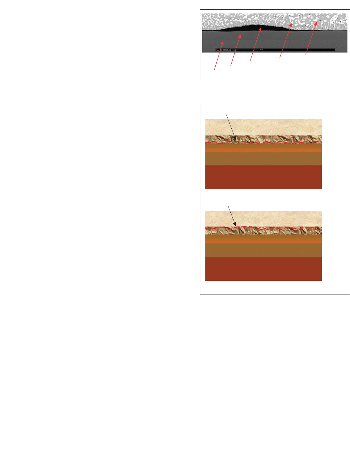
failure modes have occurred in recent years. The first fail-
ure mode is a nonwetting or dewetting condition referred to
as ‘‘black pad.’’ Figure 5-4 shows the location of crack
constituting a black pad related failure. The failure is
between nickel and Ni-Sn intermetallic (not between the
ball and Ni-Sn intermetallic).
The second failure mode is an interfacial fracture that is
associated with mechanical stress and the failure will occur
between the BGA ball and Ni-Sn intermetallic. Figure 5-5
shows an illustration to highlight the differences between
the two failure modes and the location of their occurrence.
Results from industry consortia and studies by individual
companies suggest that ‘‘black pad’’ is caused by an
aggressive attack (hyperactive corrosion) of the electroless
Ni plating during the immersion Au plating process. The
gold ions from the plating solution attract electrons from
the metallic nickel surface as they plate out as the gold
metal; in return, a nickel ion is released to the bath. Due to
certain microstructure features, such as grain boundaries
and the electrochemistry involved, the exchange does not
always occur locally, i.e., the gold can be deposited to one
feature or area and the nickel ion released from a different
feature or area. The possible consequence of this process is
that selected nickel features become attacked leaving
behind a rough and phosphorous rich layer that forms a
weak bond with solder. The affected solder joints do not
form a robust mechanical bond with the PWB, and as a
result, the solder joints fail with a relatively small applied
force, revealing lands with little or no solder left on them.
The exposed nickel surface on the land is smooth with an
Cu
Ni
Crack
Ni-Sn IMC
BGA Solder Ball
IPC-7095c-5-4
Figure 5-4 Black Pad Related Fracture Showing Crack
Between Nickel & Ni-Sn Intermetallic Layer
Crack Interface
Solder
Ni-Sn IMC
Ni-P
Ni
Cu
(a)
(b)
Solder
Ni-Sn IMC
Ni-P
Ni
Cu
Crack Interface
IPC-7095c-5-5
Figure 5-5 Crack Location for a) Black Pad Related Failure
and (b) Interfacial Fracture When Using ENIG Surface
Finish
January 2013 IPC-7095C
43
Copyright IPC-Association Connecting Electronics Industries
Provided by IHS under license with IPC
Not for Resale
No reproduction or networking permitted without license from IHS
--`,,```,,,,````-`-`,,`,,`,`,,`---
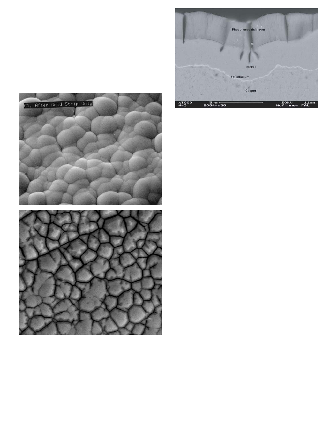
appearance varying from grey to black in color, which is
where the term ‘‘black pad’’ comes from (see Figures 5-6
and 5-7). SEM analysis shows a distinctive nickel nodular
structure similar to ‘‘mud cracks.’’ EDX indicates high
amounts of phosphorous and nickel and low amounts of
tin. Occurrence of the ‘‘black pad’’ condition does not
appear to be sufficiently common to advise against use of
electroless nickel/immersion gold as a surface finish.
Assemblers using PCBs with this finish should be aware of
the potential problem, learn to recognize it, and take cor-
rective action.
Recent analysis indicates that the interfacial fracture of the
solder joint happens between the nickel-tin intermetallic
layer and the BGA ball, or under a high level of both
applied strain and strain rate even if hyperactive corrosion
does not take place. Failures have occurred under a variety
of laboratory testing conditions including bending,
mechanical shock, and thermal cycling. Data indicates that
increasing the strain rate shifts the failure mode to an inter-
facial fracture of the solder joint. Therefore, interfacial fail-
ure may occur under a reduced strain if the strain rate is
high enough. Currently there is no industry specification
that quantitatively assesses the mechanical strength of
assembled BGA components on any surface finish.
5.3.3.2 Electrolytic Nickel/Electroplated Gold Another
version of a nickel/gold combination is the electrolytic
nickel/electroplated gold surface finish. This plating is
similar; however, it results in a different grain structure
from electroless nickel/immersion gold, and does not
exhibit the ’black pad’ joint cracking phenomenon. Electro-
lytic nickel/electroplated gold is applied after pattern plat-
ing and most often before solder mask, and therefore car-
ries some risk of surface contamination. Solder mask
applied over electrolytic nickel/electroplated gold exhibits
lower solder mask adhesion than other surface finishes.
This can create problems during assembly of BGAs, espe-
cially during rework. If the solder mask dams covering the
traces between BGA lands and vias peel off, solder will
flow from the BGA lands into the vias and cause insuffi-
cient or open solder joints.
Electrolytic nickel/electroplated gold PCBs have a shelf
life of 12 months. It is compatible with SMT, BGA and
through-hole components and it is wire-bondable. Typi-
cally, it can withstand 4 to 5 heating cycles without affect-
ing solderability. Electrolytic nickel/electroplated gold is
compatible with tin/lead and lead-free solders. It provides
a flat surface which reduces stencil printing and component
coplanarity issues.
Another concern is that it can be difficult to control the
gold thickness across the board. The gold may be too thin
(i.e., in areas with dense circuitry) or the gold may be too
thick (i.e., in isolated circuits). This latter situation may
lead to gold embrittlement due to excessive gold (>3%) in
Figure 5-6 Typical Mud Crack Appearance of Black Pad
Surface
Figure 5-7 A Large Region of Severe Black Pad with
Corrosion Spikes Protruding into Nickel Rich Layer
through Phosphorus Rich Layer Underneath Immersion
Gold Surface
IPC-7095C January 2013
44
Copyright IPC-Association Connecting Electronics Industries
Provided by IHS under license with IPC
Not for Resale
No reproduction or networking permitted without license from IHS
--`,,```,,,,````-`-`,,`,,`,`,,`---
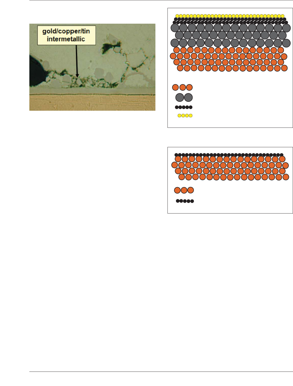
the solder joints. Gold embrittlement creates weak solder
joints that will eventually fail (see Figure 5-8).
5.3.3.3 Electroless Nickel/Electroless Palladium/
Immersion Gold (ENEPIG)
The electroless nickel/
electroless palladium/immersion gold process is similar to
ENIG except it uses a palladium metal layer that is depos-
ited after the nickel layer prior to the final gold layer. The
palladium layer is much harder than gold, providing added
strength to the surface finish for wire-bonding while pro-
tecting the underlying nickel from oxidation. The ENEPIG
structure is illustrated in Figure 5-9. ENEPIG is not widely
available from PCB suppliers and it is not widely used by
PCBA assemblers.
This finish is compatible with SMT, BGA and through-hole
components and it is wire-bondable. Nickel/gold finishes
typically can withstand 4 to 5 heating cycles without
affecting solderability. ENEPIG-coated PCBs have a shelf
life of 12 months. It provides a flat surface which reduces
stencil printing and component coplanarity issues. The high
plating temperatures and low pH of the nickel/palladium/
gold plating process can be incompatible with some solder
masks.
ENEPIG is best suited for lead-free soldering. Studies have
shown that ENEPIG does not produce very reliable tin/lead
solder joints. Pd cannot form an alloy with lead. The non-
alloyed lead disrupts the IMC formation. As Pd is intro-
duced into the Ni3Sn4 layer, it aggregates into distinctive
clusters (away from lead) creating a nonuniform IMC
layer. The excessive growth and lack of uniformity of the
IMC leads to poor reliability when ENEPIG is used with
tin/lead solder.
5.3.3.4 Direct Immersion Gold (DIG) DIG is a finishing
process that can directly deposit gold onto the copper sur-
face by utilizing an electroless plating process. A graphic
representation is shown in Figure 5-10. It is possible to
directly deposit gold on the copper surface with excellent
coverage. The main gold depositing reaction is an auto-
catalytic rather than displacement. Solderability is good
when the gold film thickness is within the range of 30 to
80 nm; however, underlying copper roughness can affect
solder wetting. Good wire-bonding characteristics can also
be derived from deposits plated by a neutral pH, auto-
catalytic type heavy electroless gold plating bath on top of
the flash gold. DIG is not widely available from PCB sup-
pliers, and it is not widely used by PCBA assemblers.
DIG typically can withstand 3 to 4 heating cycles without
affecting solderability. Solder mask compatibility is usually
not an issue. DIG coated PCBs have a shelf life of 9 to 12
months. It provides a flat surface which reduces stencil
printing and component coplanarity issues. DIG may be
best suited for tin/lead soldering applications (one reason it
is not widely used). Lead-free solder results are usually
inferior (in terms of solderability and wetting) compared to
tin/lead solder.
5.3.3.5 Immersion Silver The immersion silver finish is
produced by the selective displacement of copper atoms
with silver atoms on the exposed metal (copper) surface of
Figure 5-8 Gold Embrittlement
Copper Surface Cleaned and Microetched
Electroless Ni 5 µm (200 microinches)
Electroless Pd 0.06 µm (2.4 microinches)
Immersion Au 0.03 µm (1.2 microinches)
IPC-7095c-5-9
Figure 5-9 Graphic Depiction of Electroless Nickel/
Electroless Palladium/Immersion Gold
Copper Surface Cleaned and Microetched
Immersion Gold 0.06 µm (2 microinches)
IPC-7095c-5-10
Figure 5-10 Graphic Depiction of Directed Immersion
Gold
January 2013 IPC-7095C
45
Copyright IPC-Association Connecting Electronics Industries
Provided by IHS under license with IPC
Not for Resale
No reproduction or networking permitted without license from IHS
--`,,```,,,,````-`-`,,`,,`,`,,`---