IPC-7095C-2013.pdf - 第99页
7.1.7.1 Flux Residues that Require Cleaning (Clean) Those residues that require cleaning can be separated by the chemicals necessary to remove the residue, typically either solvent/surfactant, basic water , or deionized …

to the solder profile due to nonuniform heating (wide band
width). Note too that consistent problems may also be
related to paste quality and land pattern design.
Once the program is found to give the desired results
(assuming design and other material variables have been
optimized), document the program. After this point, no
changes should be allowed in the program and the result-
ing profile.
7.1.5 Material Issues Flux has two key attributes. First,
it must remove contamination and, second, it must protect
the solderable surfaces after contamination removal. A
common mistake is to use a time/temperature profile that
consumes the flux before the solder melts. Ideally, the flux
would be consumed just as the solder begins to melt. Acti-
vation time should range from 90 to 120 seconds. Flux
usually becomes active at around 130°C for tin lead solder
pastes. Typically, solder paste activation for lead-free sol-
der will be higher, in the 150°C range; however, it is rec-
ommended to work with your solder paste supplier for rec-
ommendation on that specific solder paste.
Components can be damaged by the incorrect application
of heat. All components have a heat exposure limit. Most
tin/lead surface mount components should tolerate a peak
temperature of 220°C for up to 60 seconds. Lead-free
BGAs will be rated to a higher temperature which is
approximately 240-260°C. Thermal shock, caused by the
rapid application of heat, can crack certain components.
However, since the peak temperature of reflow ovens var-
ies, the intent is to heat the solder in a controlled estab-
lished profile to a solder joint temperature of 210-220°C
for tin lead products and for 235-245°C for lead-free
products.
Component lead finish will affect solderability. There are a
number of lead finishes being used today, including tin/
lead, gold, tin and palladium. It is important to select a flux
and solder alloy that works well with the lead finish being
used.
7.1.6 Vapor Phase Vapor phase reflow can be operated
as a single fluid system or a two fluid system, utilizing a
primary and a secondary fluid. The process was developed
using the two fluid approach in batch equipment; but mod-
ern in-line systems are normally operated with only one
fluid. Whichever system is used, the maximum temperature
reached by assemblies in vapor phase (VP) reflow depends
on the choice of the primary fluid. Primary fluids are avail-
able in a number of temperature ranges, with 218-222°C
being common with tin lead products and 235-245°C for
lead-free products. While all the primary fluids can be
classed as perfluorocarbons, the basic structure (amine,
cyclic or ether) will determine the key properties of in-use
stability, solder paste chemicals solubility, and overall
process economics. The choice of a fluid is normally based
on the melting point of the solder alloy to be reflowed.
For the range cited, the lower temperatures are suitable for
the typical tin/lead or tin/lead-silver alloys used for stan-
dard attachment processes. The upper end of the range will
permit reflow of high lead alloys, which are used to attach
pins to PGA packages. Users faced with reflow of a spe-
cialty alloy have been successful in mixing two primary
fluids to tailor a vapor phase system for a specific stable
boiling point. Higher temperatures will permit shorter
times, which may be advantageous with some solder
pastes.
The primary vapor phase should be inert and not introduce
contaminants that must be removed later. Solder paste
chemicals that dissolve in the fluid are carried in the high
boiling vapor then deposited on the surface of the boards.
Such residues tend to be difficult to remove. Minimizing
solder paste residue in the primary fluid will maximize the
lifetime of the fluid, prevent boiling point elevation due to
dissolved paste ingredients, and simplify cleaning.
The secondary vapor blanket was originally CFC-113, a
lower boiling fluorinated material, which formed a low cost
sacrificial ‘‘lid’’ over the more costly primary fluid. The
constant exposure to the high boiling primary fluid at the
interface of the two fluids could cause the secondary fluid
to undergo thermal decomposition at the interface, generat-
ing HCl (hydrochloric) and HF (hydrofluoric) acid vapors.
These corrosive vapors often attacked the soldering equip-
ment over time. While in theory the vapors could be
absorbed in flux residues and cause problems for high reli-
ability products, this was rare in comparison to the attack
on the equipment. With the phase out of CFC-113, a low
boiling perfluorocarbon was introduced to replace it. This
second generation secondary blanket fluid was more stable
than CFC-113 for prolonged exposure to the high boiling
vapor phase fluids.
As surface mount technology grew, most users converted
to the higher throughput in-line machines, which used the
single fluid approach. Defluxing after vapor phase reflow
should be done with either a bipolar solvent formulation or
include an aqueous cleaning formulation that can ensure
removal of all the solder paste residues, with the choice of
cleaning process based on the composition of the solder
paste. Secondary factors influencing the decision would be
compatibility, and the component to PWB surface spacing.
In addition, most companies gave serious thought to con-
sidering the potential chemical loss from using this type of
equipment since many perfluoro compounds are very long-
lived global warming compounds.
7.1.7 Cleaning vs. No-Clean The selection of the solder
paste/flux technology has many implications. The two
basic types are materials where the residues require clean-
ing or can be left on the PCA without causing damage.
IPC-7095C January 2013
84
Copyright IPC-Association Connecting Electronics Industries
Provided by IHS under license with IPC
Not for Resale
No reproduction or networking permitted without license from IHS
--`,,```,,,,````-`-`,,`,,`,`,,`---

7.1.7.1 Flux Residues that Require Cleaning (Clean)
Those residues that require cleaning can be separated by
the chemicals necessary to remove the residue, typically
either solvent/surfactant, basic water, or deionized water
cleanable. Selection of a cleaning solvent should follow a
careful evaluation of technical, economic, and environmen-
tal considerations.
In general, cleaning under BGAs is difficult because the
tight gap between the board and components may entrap
flux which may be difficult to remove during cleaning.
Entrapped flux residues that require cleaning are typically
highly corrosive so this situation can lead to serious reli-
ability concerns. However, if proper care is taken in select-
ing the cleaning processes and equipment, and if the sol-
dering and cleaning processes are properly controlled,
cleaning under BGAs can be successful. In addition, if
no-clean pastes are used, the stencils are required to be
cleaned to ensure good printing. It does need to be empha-
sized, however, that good washer process control is essen-
tial when using aggressive water-soluble fluxes.
When establishing a cleaning process for water-cleanable
solder pastes, it is necessary to verify cleanliness specifi-
cally with low profile BGAs or CSPs, and BGA connec-
tors. It is common to utilize a method such as surface insu-
lation resistance (SIR) to verify that flux residues are
completely removed between the BGA balls and to estab-
lish your cleanliness process settings. Other methods such
as ion chromatography or ionography are recommended to
be used to monitor the process after qualification.
7.1.7.2 Flux Residues that Do Not Require Cleaning (No-
Clean)
The use of no-clean fluxes has increased due to
the environmental concerns of using fluxes that require
cleaning, the disposal of used solvents and the cost of the
cleaning equipment. However, no-clean is not a drop-in
process. No-clean fluxes are generally not as active as other
types of flux and hence the soldering results may be less
than desired unless adequate steps are taken. Some
no-clean fluxes require nitrogen reflow environments to
produce acceptable results; however, most currently avail-
able no-clean fluxes can be reflowed in air.
No-clean flux residues must be sufficiently inert so that
they will not damage the PCB or components. These resi-
dues are often mildly ionic and/or acidic and can poten-
tially cause product failure. The possible failure modes
caused by those residues include:
1. Corrosion of the PC board.
2. Shorting between metal traces due to dendritic growth.
3. Functional degradation of the ICs due to ionic contami-
nation diffusing into the active junctions of the die.
The first two failure modes are surface phenomena. The
effects can be detected on the board surface, and the incu-
bation time is relatively short. These failure mechanisms
are detected with the surface insulation resistance (SIR)
test or the electrochemical migration test (ECM). The third
failure mode depends on how long it takes for the external
ions, if any, to diffuse through the package encapsulation
into the die area. Once these foreign ions reach the silicon
die, they may impact its function. The diffusion time is
usually on the order of years in a normal operating envi-
ronment. Typically, some form of acceleration testing, such
as SIR or ECM, is required in order to measure this effect
within a reasonable test period. In addition, all no-clean
fluxes used on a PCA such as solder paste, wave solder flux
and even rework fluxes can all remain on the PCA and can
become mixed. It is recommended that these fluxes be
tested in combination, as well as individually, to under-
stand the complete cleanliness picture.
7.1.8 Package Standoff The package standoff is one of
the prime parameters determining the reliability of the
BGA solder joints. Package standoff for a BGA is defined
as the distance between the land on the bottom of the pack-
age substrate and the land on the top of the board surface.
This distance varies depending on the type of solder ball:
the high lead ball type stays a fairly consistent size; the
eutectic solder ball reduces the package standoff height.
This is also known as ball collapse height. For example,
when 1.27 mm tin/lead BGA is soldered on the package,
it collapses 0.1 mm and when it is soldered on the board,
the balls ‘‘collapse’’ additional 0.2 mm. So overall, for
1.27 mm ball you can expect 0.25 mm to 0.30 mm reduc-
tion from the pre-reflowed value. The high lead and copper
balls do not collapse because they do not melt. The stand-
off height on lead-free BGAs should be verified during the
set up of your process. It is recommended to establish the
process to reproduce the standoff height for specific com-
ponents.
Factors that determine the post-reflow BGA package stand-
off from the board include the BGA package weight, the
ball size, the ball material, the land size and land configu-
ration (solder mask defined or nonsolder mask defined).
Standoff height decreases with increased package weight.
However, for packages with a large ball count, the package
weight may have less effect on the standoff height. One
study on the relationship between these two parameters
discovered that increasing the package weight by 5X
decreased the standoff height by only about 0.05 mm for a
615 ball, 1.27 mm ball pitch BGA package.
Larger ball sizes will lead to larger package standoff
heights due to the larger volume of solder in each ball.
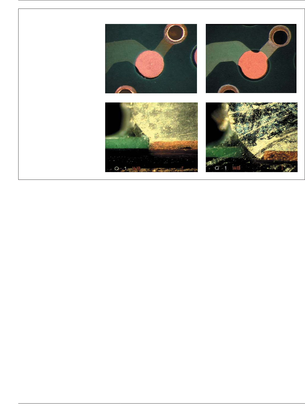
Standoff heights are inversely proportional to the land
diameters. For nonsoldermask defined (NSMD) lands, a
solder mask relief around the land may reduce the standoff
height, because the solder will wet out along the conduc-
tors as well as along the edges of the land. This is shown
in Figure 7-10.
January 2013 IPC-7095C
85
Copyright IPC-Association Connecting Electronics Industries
Provided by IHS under license with IPC
Not for Resale
No reproduction or networking permitted without license from IHS
--`,,```,,,,````-`-`,,`,,`,`,,`---
7.2 Post-SMT Processes
7.2.1 Conformal Coatings
Conformal coatings are used
to protect the parts from surface moisture and thus corro-
sion. Conformal coatings should be specified to meet the
requirements of IPC-CC-830 and should be specified on
the master assembly drawing. When UL requirements are
imposed, the coatings shall be approved by UL for use by
the printed board manufacturer.
The designer should be cognizant of compatibility issues.
Conformal coating is an electrical insulation material
which conforms to the shape of the circuit board and its
components. It is applied for the purpose of improving sur-
face dielectric properties and protecting them from the
effects of a severe environment. Conformal coatings are
not required on surfaces or in areas that have no electrical
conductors (see IPC-2221, Section 4.5.2).
Conformal coatings may be any of five types. The thick-
ness of the conformal coatings shall be as follows for the
type specified:
• AR - acrylic resin, 0.03 to 0.13 mm
• ER - epoxy resin, 0.03 to 0.13 mm
• UR - urethane resin, 0.03 to 0.13 mm
• SR - silicone resin, 0.05 to 0.21 mm
• XY - paraxylene resin, 0.01 to 0.05 mm
There are three primary chemical categories in use for con-
formal coatings. These are: silicone elastometers, parylene,
and other organics. All conformal coating types provide
various levels of protection from solvents, moisture, corro-
sion, arcing and other environmental factors that can jeop-
ardize the circuit operation.
Conformal coatings may also be used in greater thicknesses
as shock and vibration dampening agents. This type of
application brings with it the risk of mechanical stress to
glass and ceramic-sealed parts during cold temperature
excursions. Using this material may require the use of buf-
fer materials.
Caution should be taken to prevent underfilling BGAs with
conformal coating materials. Testing has shown that when
completely underfilling BGAs with conformal coating
materials (other than paraxylene) solder joint fatigue fail-
ures resulted during thermal cycle testing due to ‘‘Z’’ axis
expansion. Thus, the use of conformal coating as an under-
fill is not recommended.
Conformal coating should not be confused with encapsu-
lants. Encapsulants are used primarily to protect the bare
die as a part of the chip component package. Plastic encap-
sulants provide the protection of the plastic BGA from
external sources. The compatibility issues of encapsulants
and thermal coatings are very similar.
7.2.2 Use of Underfills and Adhesives BGAs may
require the use of adhesives to further strengthen the pack-
age to PCB interconnection. In recent years the implemen-
tation of lead-free solders and the reduction in pitches has
IPC-7095c-7-10a,b,c,d
Figure 7-10 Effect of Having Solder Mask Relief Around the BGA Lands of the Board
Solder Mask Relief Around Land ~0 mm 0.75 mm
Top view of land illustrating
increase of effective land diameter
due to trace connections
Cross-sectional view of land with
solder ball joint illustrating the sol-
der wetting down the edge of the
land when there is solder mask
relief away from the land edge
IPC-7095C January 2013
86
Copyright IPC-Association Connecting Electronics Industries
Provided by IHS under license with IPC
Not for Resale
No reproduction or networking permitted without license from IHS
--`,,```,,,,````-`-`,,`,,`,`,,`---