IPC-7095C-2013.pdf - 第44页
increases beyond the T g point, the connector will tend to either bow toward the board, or bow away from the board (‘ ‘warp’ ’). The actual behavior is a function of the connec- tor geometry , connector material, and the…
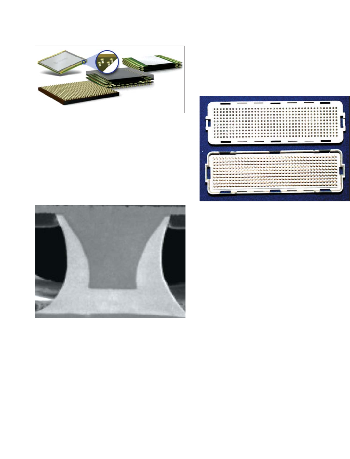
The name coined to describe this unique contact profile is
‘‘µPILR™,’’ providing significantly smaller contact feature
and finer pitch variations of 0.40 typical of the examples
shown in Figure 4-20.
When comparing the µPILR contact profile to the more
common solder ball connections, the contact geometry is
significantly smaller in both diameter and height, enabling
a much lower finished package profile. The solid copper
core contact illustrated in Figure 4-21 is slightly tapered in
shape and coated with a nickel/gold (ENIG) alloy that is
compatible with either eutectic or lead-free soldering pro-
cesses.
Circuit board assembly of the µPILR packaged device is
very typical of most surface mount processes beginning
with solder paste printing, pick-and-place and reflow
soldering. The stencil successfully used for printing is a
100 µm thick stainless steel foil with laser ablated 270 µm
square apertures. Because of the very small stencil aper-
ture, the recommended solder paste used for this appli-
cation is a Type 5 powder size. Precise placement of the
0.40 mm pitch components is critical as well. When plac-
ing ultra-fine pitch array devices, machine placement accu-
racy should be in the range of ± 20 µm to assure a reason-
ably uniform solder fillet at all contact sites.
4.5 BGA Connectors and Sockets
4.5.1 Material Considerations for BGA Connectors
The
BGA connector shown in Figure 4-22 is designed to pro-
vide a relatively low profile horizontal or parallel interface
between two circuit assemblies. The material engineered
for this application has been developed to withstand the
reflow soldering temperatures associated with surface
mount assembly and furnish a reliable interconnect in the
varying environmental conditions typical of the product’s
end use.
It is important to understand the material properties of the
connector system. During the life of the product, the circuit
board assembly will undergo many varying thermal cycles.
These thermal cycles will cause material expansion/
contraction to the assembly components, including the
BGA connector. Therefore, material selection for BGA con-
nectors is significant due to the thermal interaction of the
connector to the PCB substrate. Specifically, matching
coefficient of thermal expansion (CTE) between the BGA
connector material and the PCB substrate material are
important to the reliability of the package and the solder
joints. A close CTE match ensures that the thermally
induced stresses are minimized.
4.5.2 Attachment Considerations for BGA Connectors
Several items need to be addressed concerning the place-
ment and soldering of BGA connectors to a PCB substrate.
Some BGA connector designs do not lend themselves to a
vacuum pick-up using standard SMT nozzles. In this case,
two options are available:
1) Mechanical chuck pick-up using a custom nozzle
2) Design the BGA connector with a cap or other tempo-
rary surface so a standard vacuum nozzle can be used
Both options can be successful in production, and the best
option is highly dependent on the connector design.
Depending on the connector material, reflow profiles have
to be examined and compared to the T
g
temperature of the
connector material. When the temperature of the connector
IPC-7095c-4-20
Figure 4-20 Semiconductors Packaged with µPILR Sub-
strate
Figure 4-21 Solder Interface Between µPILR-Configured
Substrate Interposer and Circuit Board
Figure 4-22 BGA Connector
January 2013 IPC-7095C
29
Copyright IPC-Association Connecting Electronics Industries
Provided by IHS under license with IPC
Not for Resale
No reproduction or networking permitted without license from IHS
--`,,```,,,,````-`-`,,`,,`,`,,`---
increases beyond the T
g
point, the connector will tend to
either bow toward the board, or bow away from the board
(‘‘warp’’). The actual behavior is a function of the connec-
tor geometry, connector material, and the surface tension of
the connector balls to the substrate. Also included in this
analysis are the connector coplanarity requirements for suc-
cessful soldering. The material properties behavior during
reflow and the overall connector size will dictate the con-
nector ball coplanarity requirements. Typically, the copla-
narity requirements of BGA connectors are more stringent
than those of BGA IC packages, due in part to their larger
size.
4.5.3 BGA Materials and Socket Types BGA sockets
are designed to provide the interface between the processor
or other components and the circuit board. These sockets
are primarily made using a glass polymer material that can
withstand a reflow of up to 265°C. One advantage of the
glass polymer material is that it has a CTE approximately
the same as the circuit board. The interface between the
socket and circuit board utilizes BGA technology, but there
are two different designs depending upon the component
interface of the package they need to mate with. The first
is for Pin Grid Array (PGA) components, the other is for
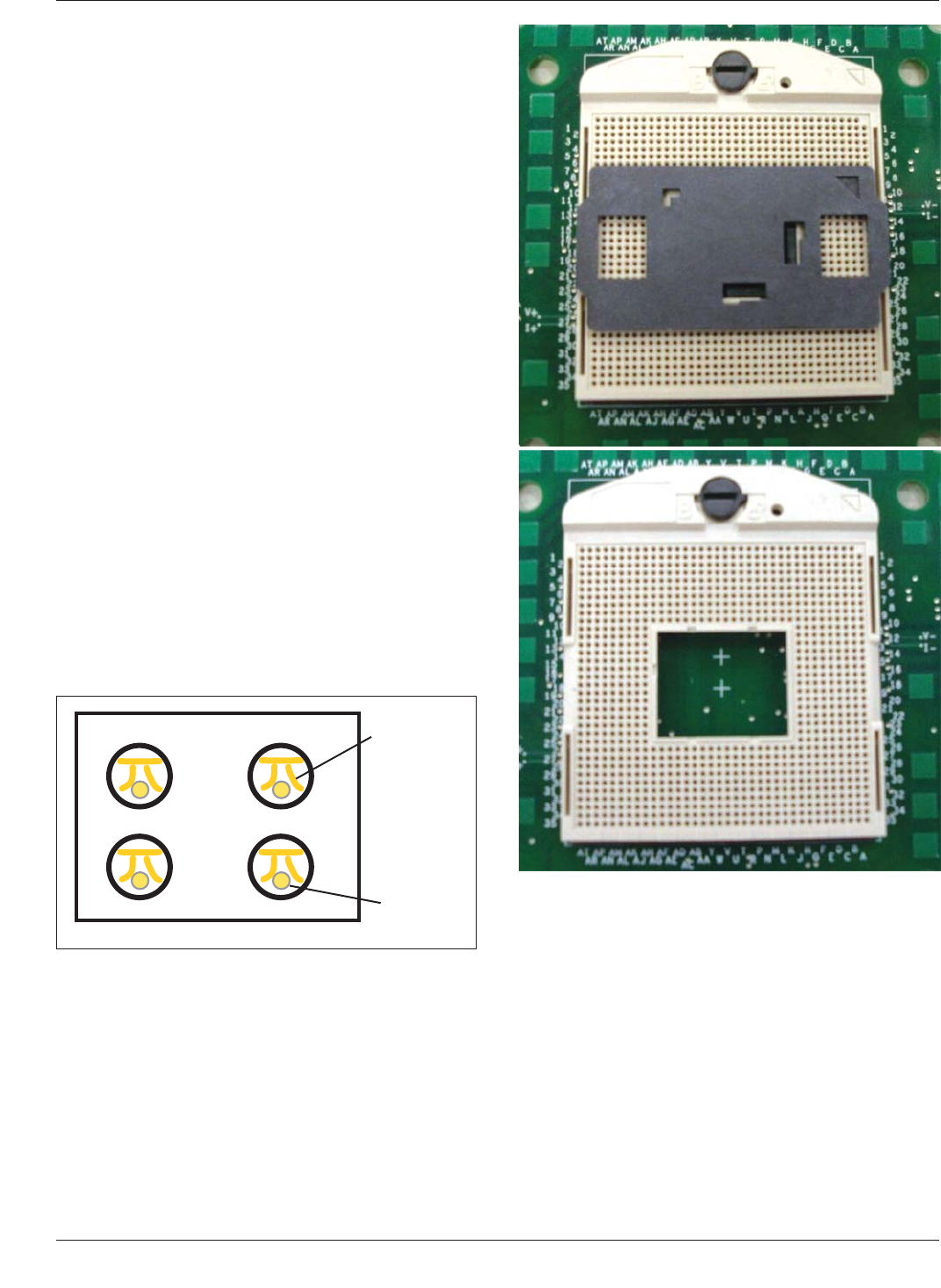
Land Grid Array components. Sockets for PGA compo-
nents are typically of a zero insertion force type (ZIF) and
utilize a cam nut that moves a cover-plate that the pins
drop through, forward pushing the pins into the contacts
and providing the load needed to make electrical contact
(see Figure 4-23 and Figure 4-24).
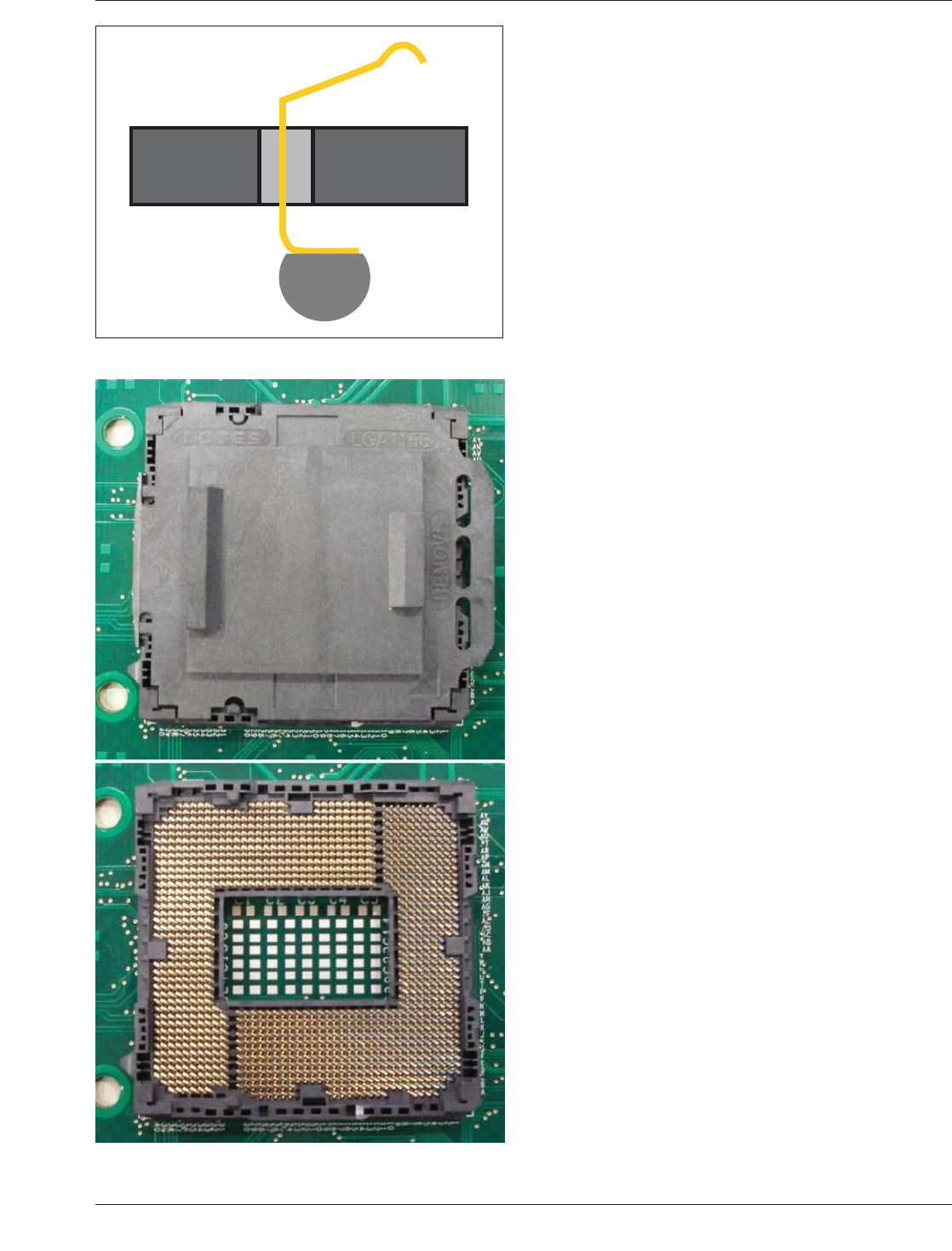
LGA sockets on the other hand use a contact bent at a pre-
cise angle allowing them to contact the land on the pack-
age. The package must have a downward load applied in
order to push the PGA Pin down against the connector
contacts. A loading mechanism is thus required and may be
built into the socket body, or in the case of an Independent
Loading Mechanism (ILM), it is installed after the socket
has been reflowed to the circuit board. The loading mecha-
nism utilizes a lever that when closed applies the necessary
downward force on the component. Both LGA and PGA
socket designs utilize a pick and place cover that snaps
over the socket. These covers serve a dual role of both
protecting the contacts and providing a flat surface for the
placement equipment nozzle to pick them up (see Figure
4-25 and Figure 4-26).
4.5.4 Attachment Considerations for BGA Sockets BGA
sockets have many similar requirements for successful
attachment as those of other BGA components. It is very
important to maintain proper ball coplanarity and control
socket warp before and during reflow. BGA socket han-
dling is even more critical than other BGA components due
to the fact that the solder ball is attached to a paddle and
not directly to a component body or substrate. If bumped,
the paddle can easily be bent, moving the solder ball out of
IPC-7095c-4-23
Figure 4-23 PGA Socket Pins
Socket
contact
PGA Pin
Figure 4-24 PGA Socket With and Without Pick and Place
Cover
IPC-7095C January 2013
30
Copyright IPC-Association Connecting Electronics Industries
Provided by IHS under license with IPC
Not for Resale
No reproduction or networking permitted without license from IHS
--`,,```,,,,````-`-`,,`,,`,`,,`---
alignment resulting in either a bridge or an open. Another
common defect type is opens that fall into the head and
pillow category. The primary cause of these open defects is
warping and is most often seen in the corner balls of the
socket. Besides having a socket that remains relatively flat
during reflow, there are several steps that can be taken to
mitigate the effect.
Processor sockets have an opening in the center to allow
for capacitors on the bottom side of the component.
Because the socket is covered by the pick and place cap,
this creates somewhat of a dead air space during reflow
causing the solder balls closest to the cavity to be cooler
than those on the outer rows. It is, therefore, important that
close attention is paid to the reflow profile minimizing the
temperature delta between the inner and outer solder balls.
Lowering the temperature delta will help minimize the
socket warp during reflow. Another step to reduce opens is
to increase the solder paste volume particularly in the areas
having the issue. It is not always practical to increase the
stencil thickness, so increasing the size of the stencil aper-
ture may be an alternative. As always, it is best to follow
the solder paste manufacturer’s recommendation when cre-
ating a reflow profile; but making sure the maximum tem-
perature, soak time, and time above liquidus are not at the
lower end can also help avoid head and pillow opens.
4.6 BGA Construction Materials
4.6.1 Types of Substrate Materials
A number of differ-
ent materials are used in the construction of BGAs. The
material choice is predicated on a number of different fac-
tors including cost, use environment, reliability require-
ments, etc. The material choice is also dependent on the
processes used in the manufacture of the BGA and the
complexity of the design required to redistribute the chip
I/O to area array format. Base materials are selected not
only by their electrical characteristics, but also their
mechanical properties. Most component manufacturers
require that the material used to redistribute the I/Os meet
a stress test identified in the JEDEC standard, JESD22, Test
Method A102B. The test consists of an exposure in a pres-
sure vessel for 168 hours. This severe accelerated stress
test permits the use of only the most robust materials for
the substrate interposer.
4.6.1.1 Bismaleimide Triazine-Glass (BT) Bismaleimide
triazine resins used in combination with glass fabric rein-
forcements are a common choice for the fabrication of sub-
strates used in BGA packages. The material is available
from a number of sources and provides good thermal per-
formance (based on a relatively high glass transition tem-
perature). In addition, the electrical properties of BT resin
(IPC-4101/30 with a T
g
range of 170-220°C) are suitable
for a great number of IC package applications.
IPC-7095c-4-25
Figure 4-25 LGA Contact Pin
Figure 4-26 LGA Socket With and Without Pick and Place
Cover
January 2013 IPC-7095C
31
Copyright IPC-Association Connecting Electronics Industries
Provided by IHS under license with IPC
Not for Resale
No reproduction or networking permitted without license from IHS
--`,,```,,,,````-`-`,,`,,`,`,,`---