IPC-7095C-2013.pdf - 第119页
For in-process control, use >35% area as the threshold with a >50% void diameter threshold. For reject-rework, use >45% area as the criteria with a >65% void diameter threshold. Use of X-ray requires some cau…
Whenever voids are observed in solder joints, they first
need to be identified in one of the above categories, in
order to determine their impact on joint reliability and to
assess corrective actions to minimize or eliminate them.
7.6 Void Measurement
7.6.1 X-Ray Detection and Measurement Cautions
Some of the real time X-ray inspection systems still in use
for the detection of solder voids employ an X-ray imaging
device that exhibits an aberration referred to in the litera-
ture as Voltage Blooming or Phosphor Blooming. Any sys-
tem using an image intensifier or flat panel detector can, in
theory, be made to bloom. However, modern, high contrast
x-ray systems, using either image intensifiers or flat panel
detectors are more than capable of providing proper
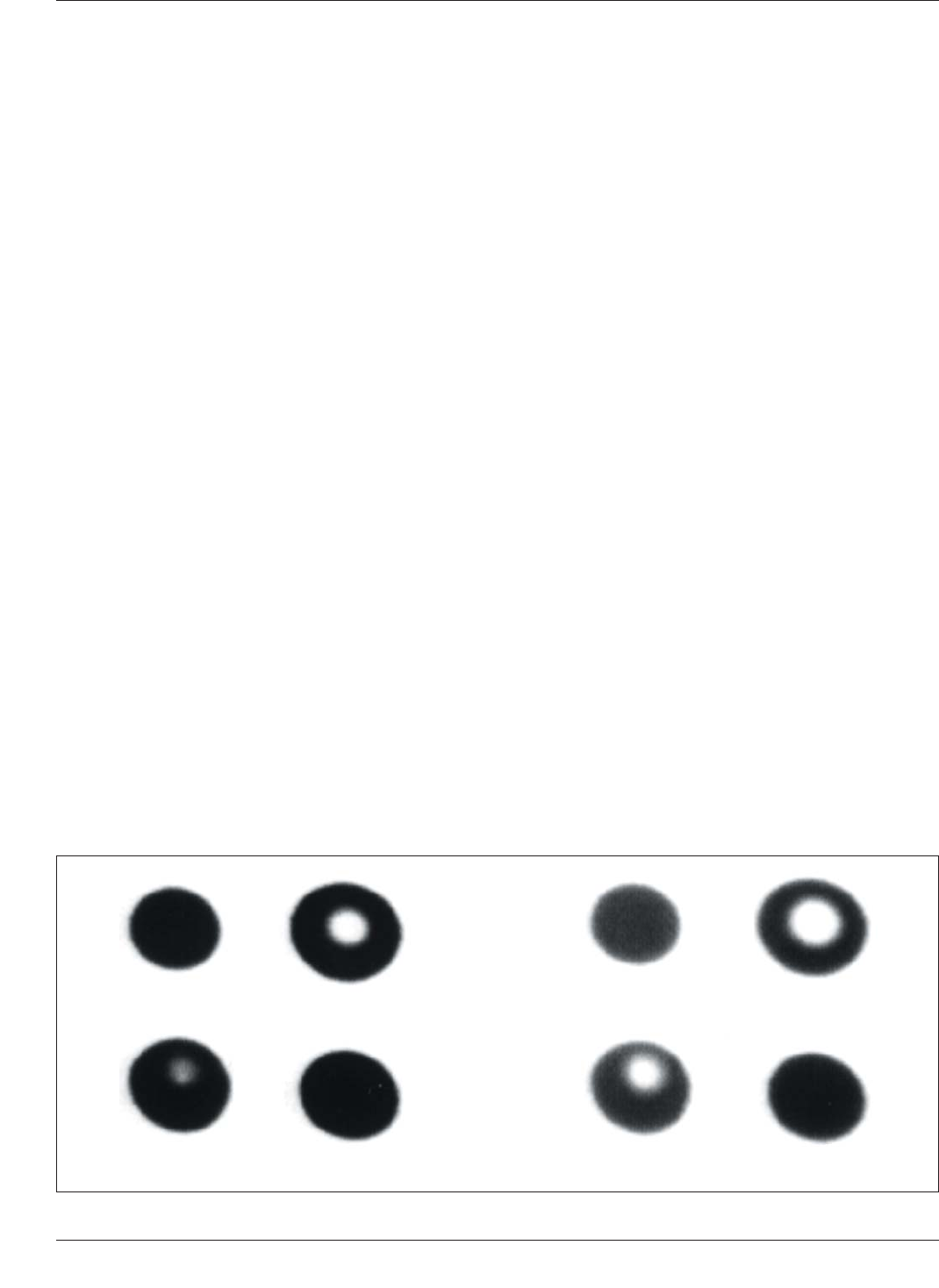
images. Figure 7-44 is an example of voltage blooming in
older systems. If it is determined that the X-ray inspection
system in use exhibits voltage blooming, the following rec-
ommendations are made to obtain a more precise measure-
ment of void size:
• X-ray film images not being subject to voltage blooming
have been found to provide a more accurate determina-
tion of void size.
• Correlation of the X-ray source voltage, to the degree of
blooming, when the actual size of a void has been deter-
mined by cross-sectioning or simulation. Note: The tonal
quality should be good enough to see a wire through the
void.
• For every voltage and current setting, the gray scale
should be reset to between 120 and 140, fora1to256
gray scale system. Normalizing gray scale will maintain
consistency between measurements.
7.6.2 Impact of Voids How many and what size of voids
should be allowable in the product before they impact the
product’s required reliability? Voids may impact reliability
by weakening the solder balls and reducing functionality
because the reduced cross-section will have lower heat
transfer and current carrying capabilities.
Large voids are more detrimental but small pre-existing
voids can merge during reflow to create large voids. The
elimination of voids, or at least a substantial reduction, is
generally preferred. The process controls to minimize void-
ing should be established during the development stage of
the process.
There are a number of studies that have shown that a small
increase in performance is observed as a result of moderate
size voids. These are typically from processes that are in
control. The increased reliability results from increased sol-
der joint height and a temporary and local retardation of
crack propagation.
X-ray inspection is required for the detection of voids in
BGA solder joints; cross-sectioning may be necessary in
order to determine the impact of the void or its location and
size.
Low cost equipment is based on transmission X-ray.
Unlike a leaded component, BGAs have solder joints that
are not only on the component’s periphery, but have inter-
nal solder joints that are not inspectable by normal visual
techniques. Higher cost equipment is based on X-ray
tomography or laminography. Both types of these systems
provide valuable techniques for void detection and location
(see 7.3.1). It is recommended that the process be qualified
for void acceptance before being released for production.
7.6.3 Void Protocol Development In many applications,
engineering teams create a void protocol which describes
the allowable voiding after the controlled experiments have
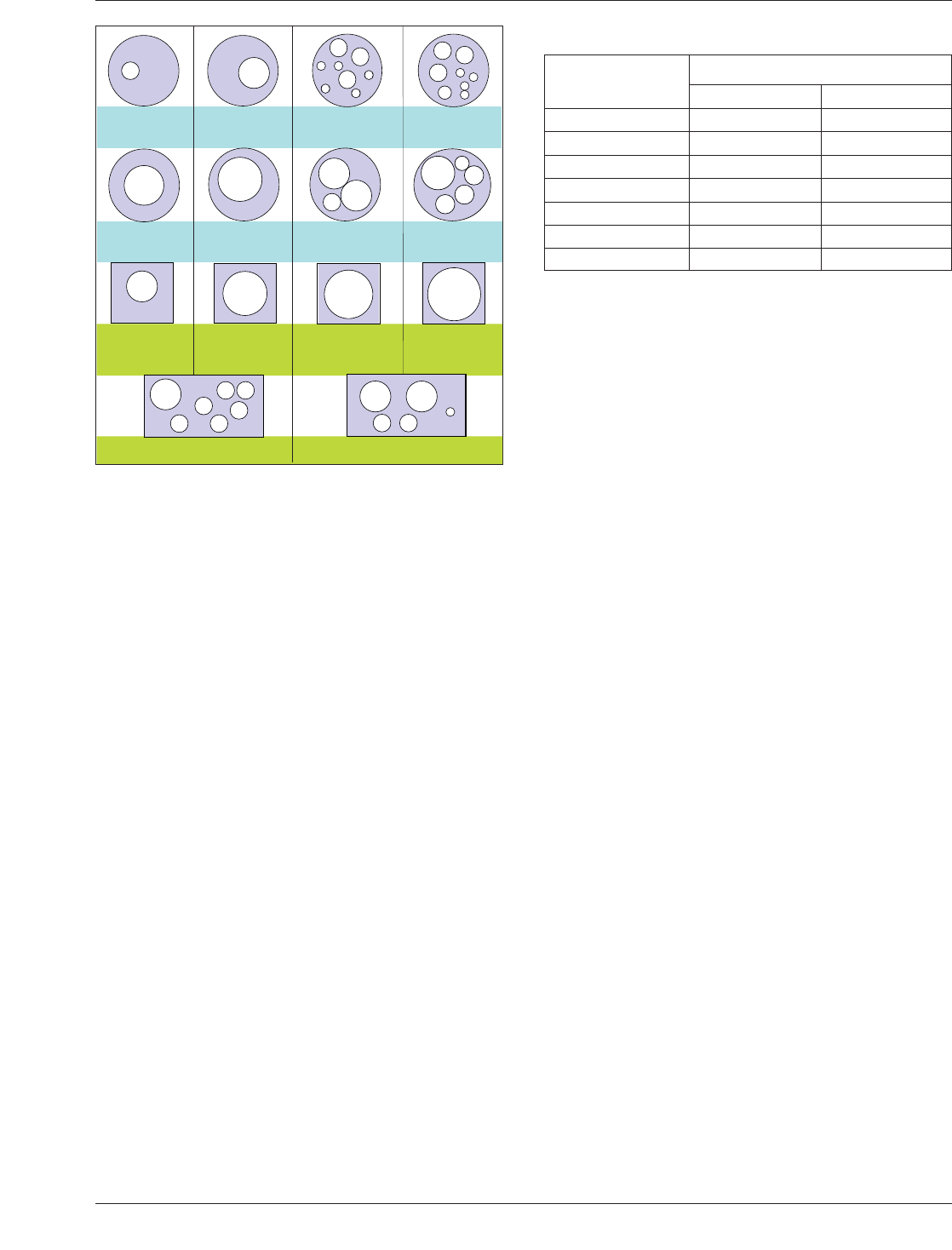
determined the characteristics of the project. Figure 7-45
shows an example of a protocol that can be established to
show the variation of void size compared to ball diameter
for various land pattern geometries.
IPC-7095c-7-44a,b
Figure 7-44 X-Ray Image of Solder Balls with Voids at 50 kV (a) and 60 kV (b)
(a) (b)
IPC-7095C January 2013
104
Copyright IPC-Association Connecting Electronics Industries
Provided by IHS under license with IPC
Not for Resale
No reproduction or networking permitted without license from IHS
--`,,```,,,,````-`-`,,`,,`,`,,`---
For in-process control, use >35% area as the threshold with
a >50% void diameter threshold. For reject-rework, use
>45% area as the criteria with a >65% void diameter
threshold.
Use of X-ray requires some caution regarding radiation
overexposure on vulnerable materials or components, as
the radiation dose from different x-ray systems can vary
widely. The implications of radiation dose to radio-
sensitive components may need to be discussed with your
component supplier and the dose rates that will be achieved
under typical x-ray inspection should be discussed with
your x-ray equipment supplier.
Although much description data is provided on identifica-
tion of voids, there is not always correlation to significant
factors related to thermal cycle life of the joint. In addition,
no data is currently available on rework vs. thermal cycle
life.
Normal area percent voids is 15 ± 10% of the projected
area.
Note: Voids at ~30% warrant process-control attention.
Voids >50% warrant rework (see Section 7.5).
Considering a 0.20 mm diameter void as an example, Table
7-7 lists the void percentages for different ball sizes. The
percentage void diameter detectable becomes larger as sol-
der joint size decreases; that is, 27% on a 0.75 mm joint
inflates to 67% on a 0.30 mm solder joint.
Defect determination is made by the product’s reliability
requirements. As an example, if the maximum allowable
void size is 31% of the solder ball diameter, the equivalent
of the void area is 9%. This can be either one void, or the
summation of many voids. Some of the newer X-ray equip-
ment use algorithms that are able to summarize the void
areas. The current algorithms for X-ray tomography do not
perform the summation of the voids.
For a single void, X-ray tomography can identify a defect
caused by a void that is greater than the pre-determined
size.
Example: If the solder ball size = 0.75 mm and the maxi-
mum allowable void size = 30% of the ball diameter, the
maximum void size at the center of the ball would be cal-
culated as follows:
30% of 0.75 mm
(0.75 mm)(0.3) = 0.225 mm maximum void diameter
When the void is not in the center of the ball and near the
land of either the board or the component, the cross-
sectional diameter of the ball will be reduced as well as the
maximum allowable size for a void.
Example: If the ball diameter at the land is approximately
equal to the land and the land size is 75% of the ball size
(25% reduction), then:
75% of 0.75 mm = 0.56 mm ball diameter at the land
30% of 0.56 mm = maximum void diameter
(0.56)(0.3) = 0.17 mm maximum void diameter
at the land
7.6.4 Sampling Plans for Void Evaluation Because of
the industry concern regarding voids, this standard attempts
to define criteria for void baseline goals and process con-
trol techniques. Everyone agrees that it makes no sense to
throw away good product, or rework product where a void
is identified without some indication as to the complexity
and the impact on reliability of that condition.
Void occurrence criteria are not based on 100% inspection,
but are accomplished through the use of sampling plans.
The sampling plan conditions are identical to those shown
in IPC-6012 and are repeated in Table 7-8. It should be
noted that the table is based on C=0. What this means is
that, as within all IPC standards, when a sample is selected,
IPC-7095c-7-45
Figure 7-45 Examples of Suggested Void Protocols
025" land 06" void
24% DIAMETER
6% AREA
025" land 013" void
52% DIAMETER
27% AREA
.020" X .030"
.010" VOID
50% DIAMETER
10% AREA
20 X 40 + 10,5,5,5,5,5,5
24% AREA
20 X 40 + 10,10,5,5,3
26% AREA
.020" X .030"
.014" VOID
70% DIAMETER
19% AREA
.020" X .030"
.016" VOID
80% DIAMETER
25% AREA
.020" X .030"
.018" VOID
90% DIAMETER
31% AREA
025" land 015" void
60% DIAMETER
36% AREA
025" land 010" void
50% DIAMETER
16% AREA
25 + 6,6,6,3,3,3,3,3
24% AREA
25 + 10,10,6
38% AREA
25 + 10,6,6,6
37% AREA
25 + 6,6,6,4,3,3,3,3
25% AREA
Table 7-7 Ball-to-Void Size Image -
Comparison for Various Ball Diameters
Solder Ball
Diameter/
X-Ray Image
Void 0.20 mm Diameter
% Void Diameter % Void Area
0.85 mm 24% 6%
0.75 mm 27% 7%
0.65 mm 31% 9%
0.55 mm 36% 13%
0.45 mm 44% 20%
0.40 mm 50% 25%
0.30 mm 67% 44%
January 2013 IPC-7095C
105
Copyright IPC-Association Connecting Electronics Industries
Provided by IHS under license with IPC
Not for Resale
No reproduction or networking permitted without license from IHS
--`,,```,,,,````-`-`,,`,,`,`,,`---

any occurrence of exceeding the characteristics for void
size shown in Table 7-7, requires 100% evaluation of the
total lot.
The appropriate corrective action may vary based on class
of product and customer requirements. The ultimate action
is to remove and replace the affected component; however,
those solutions must be carefully evaluated as the product
should have been designed to permit repair procedures that
include reevaluation.
Once a void protocol has been established as to the percent
attachment permitted, random samples should be taken
from the production units and evaluated as to compliance
with the accepted conditions identified in the protocol. The
decision as to how many samples to take depends on the
number of units being produced. A consideration should
also be given to the number of BGAs that are part of the
particular assembly.
The index value of 2.5 is a good representation that can
provide an insight into the capabilities of the process
regarding BGA assembly and the occurrence of voids. The
Level A 2.5 index can be used for evaluating commercial
product used in consumer goods and computer applica-
tions. It is also appropriate for telecommunication equip-
ment. For a Class 2 equipment where high performance
and extended life is required, and for which uninterrupted
service is desired but is not critical, and certain cosmetic
imperfections are allowed an index indicator of 1.5 should
be used.
Class 3 is for High Reliability Electronic Products and
includes equipment for commercial and military products
where continued performance or performance on demand is
critical. Equipment downtime cannot be tolerated, and
must function when required such as for life support items,
or critical weapons systems. Printed board assemblies that
contain BGAs in this class are suitable for applications
where high levels of assurance are required and service is
essential; thus, the evaluation requires a sampling of 1.0
index value.
The purpose of the index value is to define the possibility
that, although the samples reviewed all meet the defined
void protocol, there is still a statistical possibility of the
percentage shown by the index that some of the product
may not meet the conditions established. A 1.0 index for
level C requires that 13 samples be examined from a pro-
duction lot of 125 assemblies. Even if the samples all meet
the protocol, there is still a possibility that 1.0% of the lot
size do not. This relates to less than 2 assemblies and
would be a satisfactory risk in many applications.
7.7 Process Control for Void Reduction
7.7.1 Process Parameter Impact on Void Formation
In
order to establish process control for BGA assembly it is
important to understand what parameters can impact void-
ing frequency and size in board assembly process. The
voids found in solder joints after assembly are usually
called process voids, which are also known as macrovoids.
The process voids are normally caused by the evolution of
volatile ingredients of fluxes and solder pastes. However, if
big voids in solder joints are found after the SMT process,
they may not be generated during the SMT process only.
The ball attach process for attaching solder balls to the
BGA package substrates can also generate voids in the sol-
der balls. It is therefore necessary to investigate the amount
of voids within the solder balls of BGA components. This
voiding level within the balls of BGA components can be
very high. The JEDEC guideline, JESD 217, suggests the
Pre-SMT BGA voids percentage should be less than 15%.
High levels of voids within the BGA solder balls may
Table 7-8 C=0 Sampling Plan (Sample Size for Specific Index Value*)
Lot Size
Class 1 Class 2 Class 3
2.5* 4.0* 6.5* 1.5* 2.5* 4.0* 0.10* 1.0* 2.5* 4.0*
1-8 5 3 2 ** 5 3 ** ** 5 3
9-15 532853**1353
16-25 533853**1353
26-50 555855**1355
51-90 765876**1376
91-150 11 7 6 12 11 7 125 13 11 7
151-280 13 10 7 19 13 10 125 20 13 10
281-500 16 11 9 21 16 11 125 29 16 11
501-1200 19 15 11 27 19 15 125 34 19 15
1201-3200 23 18 13 35 23 18 125 42 23 18
3201-10,000 29 22 15 38 29 22 192 50 29 22
10,001-35,000 35 29 15 46 35 29 294 60 35 29
*Index Value is associated to the A.Q.L. value. If a particular product is determined to be ‘‘critical’’ by the user and a smaller index value is required, the user
shall designate the requirement in the procurement document and should state the ‘‘critical’’ requirement on the master drawing.
**Denotes inspect entire lot.
IPC-7095C January 2013
106
Copyright IPC-Association Connecting Electronics Industries
Provided by IHS under license with IPC
Not for Resale
No reproduction or networking permitted without license from IHS
--`,,```,,,,````-`-`,,`,,`,`,,`---