IPC-7095C-2013.pdf - 第138页
BGA ball and the solder paste which indicates that the paste did not reach proper reflow temperature. In some cases, the solder paste may not have coalesced. It should be noted that for most lead-free solder, the surfaces…
8.3.1 Global Expansion Mismatch The global expansion
mismatches result from differential thermal expansions of
an electronic component or connector and the printed board
to which it is attached via the surface mount solder joints.
These thermal expansion differences result from differences
in the CTEs and thermal gradients as the result of thermal
energy being dissipated within active components. Global
CTE mismatches typically range from about 2 ppm/°C for
CTE-tailored high reliability assemblies to ≥14 ppm/°C for
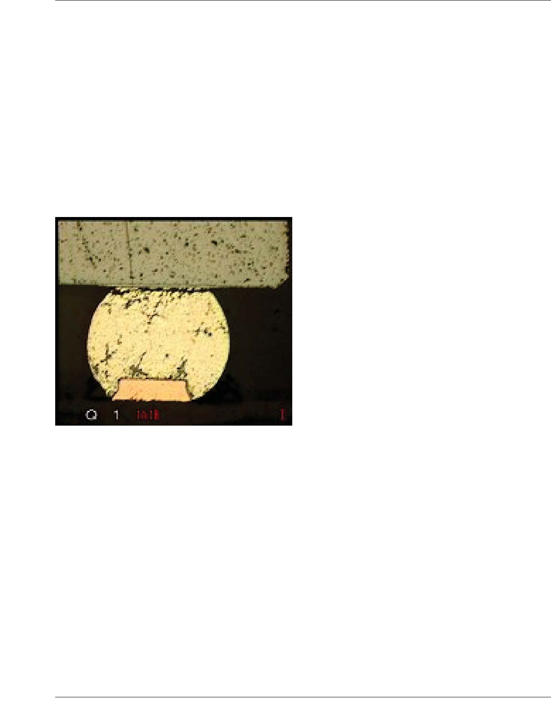
ceramic components on FR-4 printed boards. Figure 8-6 is
showing a solder joint failure due to CTE mismatch on a
wafer level CSP. The silicon die on the top expands much
less than the FR-4 substrate on the bottom. This causes
shear stress on the solder joint, which eventually fails at the
die to solder interface when subjected to temperature
cycling stresses.
8.3.2 Local Expansion Mismatch The local expansion
mismatch results from differential thermal expansions of
the solder and the base material of the component or PWB
to which it is soldered. These thermal expansion differ-
ences result from differences in the CTE of the solder and
those of the base materials from thermal excursions. Local
CTE mismatches typically range from 7 ppm/°C with cop-
per to 18 ppm/°C with ceramic and 20 ppm/°C with Alloy
42 and Kovar. Local thermal expansion mismatches typi-
cally are smaller than the global expansion mismatches,
since the acting distance, the maximum wetted area dimen-
sion, is much smaller: in the order of hundreds of microm-
eters instead of thousands.
8.3.3 Internal Expansion Mismatch In tin/lead solders,
an internal CTE mismatch results from the different CTEs
of the tin-rich and lead-rich phases of the solder. Internal
thermal expansion mismatches typically are the smallest,
since the acting distance, the size of the grain structure, is
much smaller than either the wetted length or the compo-
nent dimension - in the order of less than 25 µm.
For lead-free solders, the metallurgy is more complicated
due to the ternary or quarternary alloy composition concen-
trated at very high tin contents.
8.4 Solder Attachment Failure Failure of the solder
attachment of a component to the substrate to which it is
surface mounted is commonly defined as the first complete
fracture of any of the solder joints of which the component
solder attachment consists. Given that the loading of the
solder joints is typically in shear, rather than in tension, the
mechanical failure of a solder joint is not necessarily the
same as the electrical failure. Electrically, the mechanical
failure of a solder joint results, at least initially, in the
occasional occurrence of a short-duration (<1 µs) high
impedance event during either a mechanical or thermal dis-
turbance.
From a practical point of view, the solder joint failure is
defined as the first observation of such an event. For some
applications this failure definition might be inadequate. For
high speed signals with sharp rise times, signal deteriora-
tion prior to the complete mechanical failure of a solder
joint might require a more stringent failure definition.
Similarly, for applications which subject the electronic
assemblies to significant mechanical vibration and/or shock
loading, a failure definition that considers the mechanical
weakening of the solder joints as the result of the accumu-
lating fatigue damage might be necessary.
8.4.1 Solder Attachment Failure Classification There
are some common BGA failure signatures. These defects
can be induced during the assembly process or they could
be latent solder joint defects or failures. Such defects
and/or failures are the result of an inadequate assembly
process, defective material or excessive mechanical stress
during assembly. The defects could be a partial open or
very weak interfaces, the latent failures could be hairline
cracks, open joint with a full contact and partially lifted
land. They are difficult to detect using conventional process
verification tools such as X-ray and ICT test. They are a
major reliability concern since they can be intermittent.
Subsequently, they are tracked down following high levels
of fields returns.
8.4.2 Failure Signature-1: Cold Solder Cold solder joint
is a result of a low peak temperature during the reflow pro-
cess (<Liquidus+20°C). The Liquidus temperature of a sol-
der alloy is the temperature above which the whole solder
volume is liquid. The solder paste partially melts and will
form a cold solder joint. The joint may have a rough sur-
face and sometimes necking at the interface to the board.
The solder will appear grainy as shown in Figure 8-7 and
there will be a difference between the grain structure of the
Figure 8-6 Solder Joint Failure Due to Silicon and Board
CTE Mismatch
January 2013 IPC-7095C
123
Copyright IPC-Association Connecting Electronics Industries
Provided by IHS under license with IPC
Not for Resale
No reproduction or networking permitted without license from IHS
--`,,```,,,,````-`-`,,`,,`,`,,`---
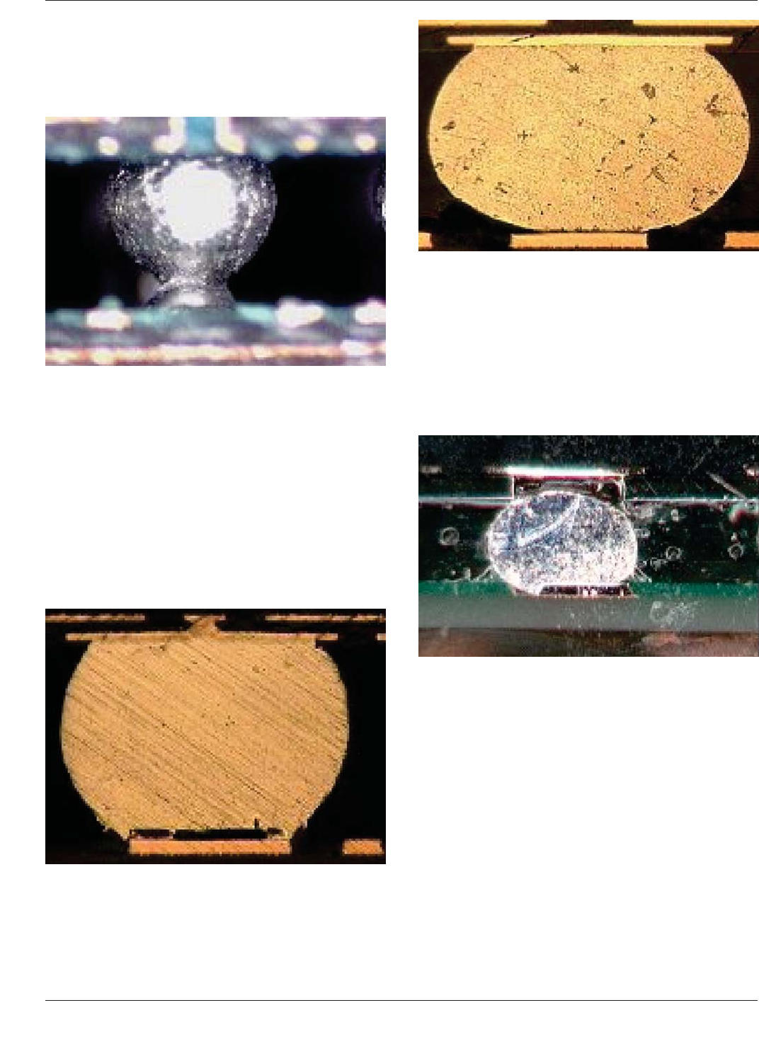
BGA ball and the solder paste which indicates that the
paste did not reach proper reflow temperature. In some
cases, the solder paste may not have coalesced. It should be
noted that for most lead-free solder, the surfaces of the sol-
der joints will appear grainy.
8.4.3 Failure Signature-2: Land, Nonsolderable Con-
tamination on the PCB land will cause nonsolderable inter-
face between the PCB land and the BGA ball. The solder
will wet to the BGA ball but not to the land. There might
be a partial or complete open with electrical contact. A
failure with this signature could be a result of faulty nickel
plating on the PCB with ENIG as a surface finish. One type
of failure, known as ‘‘black pad,’’ is shown in Figures 8-8
and another type of failure is shown in Figure 8-9. It also
could be a result of PCB supplier rework process and reap-
plying solder mask to the BGA area.
8.4.4 Failure Signature-3: Ball Drop This is an open sol-
der joint which forms between the solder ball and the BGA
component substrate. This causes the BGA ball to drop and
creates elongated solder ball with round or a flat top. Ball
drop is a failure caused by a high topside temperature dur-
ing wave solder (>Liquidus-20°C). The Liquidus tempera-
ture of a solder alloy is the temperature above which the
whole solder volume is liquid. During wave soldering, the
BGA balls are softening due to the high topside tempera-
ture. Thermo-mechanical stress is causing the balls to pull
away from the component substrate and create an open
joint as shown in Figure 8-10. Ball drop can also be caused
by high peak temperature and dwell time during reflow.
8.4.5 Failure Signature-4: Missing Ball Missing solder
ball during ball attached process or due to handling dam-
age is shown in Figure 8-11. This defect signature is usu-
ally very clear and is easy to detect with X-ray or ICT
techniques.
8.4.6 Failure Signature-5: PCB and BGA Stack War-
page
As both the package substrate and the PCB thick-
ness have become thinner with the advent of the recent
boom in handheld products, such as smart phones and tab-
lets, the magnitude of this dynamic warpage has increased.
This increase in dynamic warpage causes new, various sol-
der joint shapes.
This signature occurs when the PCB and/or BGA stack is
warping during the reflow process as shown in Figure 8-12.
For flip chip BGA Packages, the silicon die expands much
less than the package substrate laminate. This expansion
Figure 8-7 Grainy Appearing Solder Joint
Figure 8-8 Nonsolderable Land (Black Pad)
Figure 8-9 Land Contamination (Solder Mask Residue)
Figure 8-10 Solder Ball Drop
IPC-7095C January 2013
124
Copyright IPC-Association Connecting Electronics Industries
Provided by IHS under license with IPC
Not for Resale
No reproduction or networking permitted without license from IHS
--`,,```,,,,````-`-`,,`,,`,`,,`---
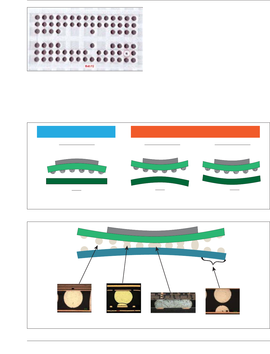
mismatch creates a generalized ‘‘bi-metallic strip’’ effect
when the BGA package is heated and cooled during the
SMT Reflow Soldering process. This effect creates a
‘‘dynamic’’ warpage of the package. The FCBGA package
may become concave in shape, with negative (-) warpage,
when heated to the SMT reflow temperature, above 220°C,
but then become less warped when cooled down after exit-
ing the reflow soldering oven. Similarly, the PCB also
exhibits dynamic warpage behavior and may go from a
being relatively flat to becoming convex or concave (as
shown in Figure 8-12).
The FCBGA package and board warpage can affect the
solder joint formation. Various solder joint defects can
occur during SMT reflow soldering due to the increase in
PCB and/or BGA stack warpage, under un-optimized SMT
process. These include Head-on-Pillow (HoP), Head-on-
Pillow Open which is similar to HoP but the solder ball
does not make any contact with the solder on the PCB
land, Non-wet Open (NWO) where there is no solder on
the PCB land and Solder Bridging. Figure 8-13 depicts the
case of a severely warped PCB and BGA stack causing
these solder joint defects across the ball array of the pack-
age. SMT process optimized solutions are listed in Section
9.4.
Figure 8-11 Missing Solder Ball
IPC-7095c-8-12
Figure 8-12 Example of Dynamic Warpage of Flip Chip BGA Packages and PCBs
At Room Temperature / Before
Reflow Soldering
PCB
Relatively Flat
PCB
Positive (+) Warpage
Convex in Shape
PCB
Negative (-) Warpage
Concave in Shape
When Heated to Reflow Temperatures
(OR)
FCBGA Package
Positive (+) Warpage
Convex in Shape
FCBGA Package
Negative (-) Warpage
Concave in Shape
FCBGA Package
Negative (-) Warpage
Concave in Shape
P
a
c
k
a
g
e
S
u
b
s
t
r
a
t
e
S
i
l
i
c
o
n
D
i
e
IPC-7095c-8-13
Figure 8-13 Example of a Severely Warped BGA Package and PCB After Reflow Soldering in an Un-Optimized SMT Process
Die
Package Substrate
Board
Non-Wet Open
(NWO)
Head-on-Pillow
(HoP)
Solder bridging Head-on-Pillow
(HoP) Open
January 2013 IPC-7095C
125
Copyright IPC-Association Connecting Electronics Industries
Provided by IHS under license with IPC
Not for Resale
No reproduction or networking permitted without license from IHS
--`,,```,,,,````-`-`,,`,,`,`,,`---