IPC-7095C-2013.pdf - 第34页
4.3.1.3 Fine Pitch Rectangular BGA Package JEDEC Publication JEP95, Section 4.6 defines a fine-pitch, rectan- gular ball grid array (FRBGA) has an array of metallic balls on the underside of the package. The substrate or c…
4.2.2 Flip Chip The flip chip (or direct-chip-attach)
design eliminates the need for wires and die attach. In this
design, the pre-bumped die is flipped circuit side down and
the lands on the circuit side of the die are brought into
contact with corresponding lands on a substrate using sol-
der or conductive adhesive. The die bond pads, however,
are not immediately compatible with either solder or con-
ductive adhesive attachment processes. Solder bumping
with a solder compatible alloy composition before the die
wafer is sawed is one of the most common procedures. The
solder material and the bumped-pad structure materials are
chosen to optimize electrical and mechanical connection
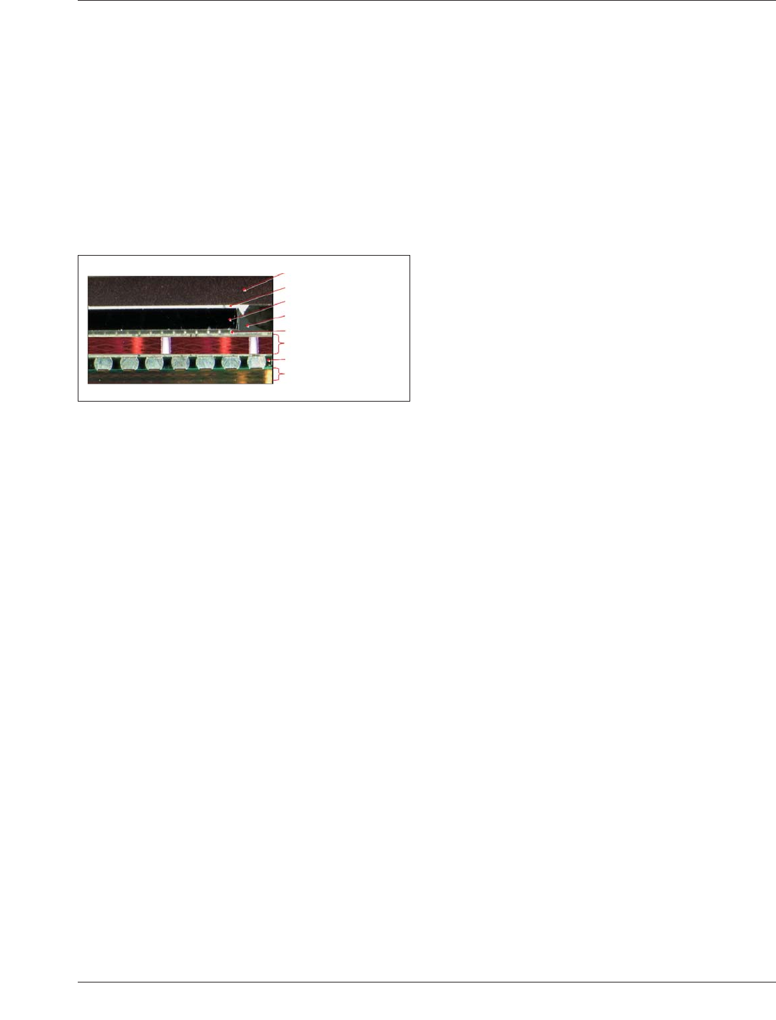
typical of that shown in Figure 4-4.
Conductive adhesive or polymer attachment can be adapted
as well; however, the die bump contact may require a
‘‘noble’’ alloy that is compatible with the conductive alloy
particles in the adhesive. This alloy bump or ball can be
applied to the die bond pads by plating or ball bonding
processes. If a solder or an isotropic conductive adhesive is
used, the gap between the die and the substrate may require
an under-die-filling with epoxy to ensure mechanical integ-
rity of the die-to-substrate interface. Use of an anisotropi-
cally conductive material eliminates the need for added
underfill. After attaching the die to the substrate, it is typi-
cally encapsulated, coated, or over-molded for protection.
4.3 Standardization Standardization of BGA packaging
has considered a number of physical variables including
the diameter of the individual ball, the positional accuracy
of the ball in relationship to a true position within the com-
ponent outline.
4.3.1 Industry Standards for BGA For more detail
regarding package variation, mechanical feature dimen-
sions and allowable physical tolerances, refer to the follow-
ing JEDEC developed guidelines for BGA packaging.
4.3.1.1 BGA Package JEDEC Publication JEP95,
Section 4.14 defines a ball and column grid array package
family. A ball grid array (BGA) package or column grid
array (CGA) is a square or rectangular 1.50, 1.27, and
1.00 mm pitch package with an array of metallic balls or
columns on the underside of the package. The main body
of the package has a metallized circuit pattern applied to a
dielectric structure. To this package body, the semiconduc-
tor die(s) are attached to either the top or bottom surface.
On the underside of the dielectric is an array pattern of
metallized balls/columns which form the mechanical and
electrical connection from the package body to a mating
feature such as a printed circuit board. The surface that
contains the die may be encapsulated by various techniques
to protect the semiconductor.
4.3.1.2 Fine Pitch BGA Package JEDEC Publication
JEP95, Section 4.5 defines an FBGA package as a reduced-
pitch (<1.00 mm) version of a BGA package. The carrier
body of the package has a metallized circuit pattern applied
to a dielectric structure. One or more semiconductor
devices are attached to either the top or the bottom surface
of this dielectric carrier. On the underside of the dielectric
carrier is an array pattern of metallized balls, which form
the mechanical and electrical connection from the package
body to a mating feature such as a printed circuit board.
The surface that contains the die may be encapsulated
by various techniques to protect the semiconductor.
The requirements for a square FBGA package family
allows three optional contact pitch variations: 0.50, 0.65,
and 0.80 mm and defines four device profile (height) varia-
tions as well. Additionally, a 0.75 mm contact pitch has
been included on the Die Size BGA (DSBGA) package
guideline, thus providing four pitch variations for the die
size device family.
The total profile height of the FBGA as measured from the
seating plane to the top of the component is >1.70 mm. The
low-profile fine-pitch ball grid array (LFBGA) is a
reduced-height version of an FBGA. The total profile
height of the LFBGA as measured from the seating plane
to the top of the component is no greater than 1.20 mm.
Thin profile fine pitch ball grid array (TFBGA) is a
reduced-height version of an FBGA with a total profile
height as measured from the seating plane to the top of the
component that does not exceed 1.00 mm and the very thin
profile fine pitch ball grid array (VFBGA) is a reduced-
height version of an FBGA with a total profile height as
measured from the seating plane to the top of the compo-
nent that is at or below 0.80 mm.
The JEDEC design guide for FBGA allows the manufac-
turer the option to increase ball diameter as the spacing or
pitch between ball contact centers increase as compared in
Table 4-1. The JEDEC FBGA and FRBGA design guide
does not support the 0.75 mm pitch; however, the industry
has registered some nonconforming parts with that pitch.
These are non-JEDEC packages.
The larger ball diameter option has been allowed to accom-
modate packages using rigid interposer structures. The
larger diameter ball may compensate, to a degree, for the
wide mismatch of the coefficient of thermal expansion
(CTE) between the silicon die and the rigid PCB structure.
IPC-7095c-4-4
Figure 4-4 Flip-Chip (Bumped Die) on BGA Substrate
Heat Spreader
Thermal Paste
Flip Chip Solder Balls
Package Substrate
BGA Solder Balls
Circuit Board
Underfill
Die
January 2013 IPC-7095C
19
Copyright IPC-Association Connecting Electronics Industries
Provided by IHS under license with IPC
Not for Resale
No reproduction or networking permitted without license from IHS
--`,,```,,,,````-`-`,,`,,`,`,,`---

4.3.1.3 Fine Pitch Rectangular BGA Package JEDEC
Publication JEP95, Section 4.6 defines a fine-pitch, rectan-
gular ball grid array (FRBGA) has an array of metallic
balls on the underside of the package. The substrate or car-
rier of the package has a rectangular shape with a metal-
lized circuit pattern applied to either or both sides of a
dielectric structure. Generally described with the same gen-
eral terms noted in the JEP95, Section 4.5, the body size
for an FRBGA is defined by the D and E dimensions.
Dimension D is the size of the body when measured paral-
lel to the major axis of the package, and dimension E is the
size measured parallel to the minor axis. Thus, for rectan-
gular packages, D will have a larger value than E.
4.3.1.4 Die Size BGA Package JEDEC Publication
JEP95, Section 4.7 defines a die-size ball grid array
(DSBGA) package. A Die-size Ball Grid Array has an array
of metallic balls on the underside of the package. The sub-
strate or carrier of the package may have a square or rect-
angular shape with a metallized circuit pattern applied to
either or both sides of a dielectric structure. The semicon-
ductor die is attached to the top surface of this dielectric
carrier. On the underside of the dielectric, the array pattern
of metallized balls provides the mechanical and electrical
connection from the package body to the next level com-
ponent such as a printed circuit board. The surface to
which the die is attached may be encapsulated by various
techniques to protect the semiconductor. The size of the
substrate or carrier is as close to the die size as practically
possible.
A ‘‘die-size’’ ball grid array (DSBGA) is a type of BGA
package where the body size is defined to coincide as
closely as possible with a specific die size. This package is
sometimes called a ‘‘real chip-size’’ BGA or CSP. The
dimensions of the package body accommodate assembly
only of a die with a specific size, and these body dimen-
sions will change as a result of future changes in die size.
The outline of the package may be square or rectangular,
but this aspect ratio may also change as a given package is
redesigned to conform to a new die size. The aspect ratio
will likely differ for devices of the same functionality from
multiple suppliers. The controlling factor for the standard-
ization of DSBGA packages is the size and aspect ratio of
the ball array.
The D and E dimensions define the body size for a DSBGA
package. For packages with a rectangular ball matrix, the
matrix determines the orientation of the dimensions.
Dimension D is the body size measured parallel to the
major axis of the ball matrix, and dimension E is the body
size measured parallel to the minor axis of the ball matrix.
Thus for rectangular packages, D will not necessarily have
a larger value than E as would be the case for an FRBGA
package per JEDEC JEP95, Section 4.6. A DSBGA pack-
age with a square ball matrix should follow the usual
JEDEC convention where D is greater than E. The maxi-
mum values for both D and E are defined in JEDEC Pub-
lication 95 using 0.50 mm increments. The values are
determined by rounding the actual DSBGA body size
upward to the next 0.50 mm boundary. Thus, D and E val-
ues have the form y.00 or y.50 following this procedure.
The array pitch for a DSBGA package will not necessarily
be equal for the D and E matrix dimensions. When the
pitches are not equal, ball dimensions and tolerances for
the smaller of the two pitches will govern the definition of
related package dimensions and tolerances. The controlling
pitch of the array of balls on a DSBGA package is always
less than 1.0 mm. The contact pitch variations for the
DSBGA described in JEP95, Section 4.7, are 0.80, 0.75,
0.65 and 0.50 mm.
4.3.2 Ball Pitch Ball Grid Arrays are divided up into two
groups of pitches. The first group includes both plastic and
ceramic package outlines allowing 1.50, 1.27, and 1.00 mm
contact pitch variations. The second group is designated
as a fine-pitch and die size BGA package family allowing
ball contact pitch variations of 0.80, 0.75, 0.65, 0.50, 0.40,
0.30, and 0.25 mm for the die size BGA. Few component
manufacturers are currently providing parts with 1.5 mm
pitch, as the pressure is on form factor in order to keep
BGAs as small as possible and although ball pitch of
0.40 mm and less are allowed, the applications may be
limited for conventional surface mount assembly due to
difficulty in processing. Pitch plays a large role in the deter-
mination of what ball diameters can be used in various
combinations. Table 4-2 shows the characteristics of those
balls that are used with pitches of 0.5 mm through 1.5 mm
for PBGAs while Table 4-3 shows the future balls for
DSBGAs.
Table 4-1 JEDEC Standard JEP95-1/5
Allowable Ball Diameter Variations for FBGA
Ball Pitch
Ball Diameter/mm
Min. Nom. Max.
0.50 0.25 0.30 0.35
0.65 0.25 0.30 0.35
0.65 0.35 0.40 0.45
0.80 0.25 0.30 0.35
0.80 0.35 0.40 0.45
0.80 0.45 0.50 0.55
Table 4-2 Ball Diameter Sizes for PBGAs
Nominal Ball
Diameter (mm)
Tolerance
Variation (mm) Pitch (mm)
0.75 0.90 - 0.65 1.5, 1.27
0.60 0.70 - 0.50 1.0
0.50 0.55 - 0.45 1.0, 0.80
0.45 0.50 - 0.40 1.0, 0.80, 0.75
0.40 0.45 - 0.35 0.80, 0.75, 0.65
0.30 0.35 - 0.25 0.80, 0.75, 0.65, 0.50
IPC-7095C January 2013
20
Copyright IPC-Association Connecting Electronics Industries
Provided by IHS under license with IPC
Not for Resale
No reproduction or networking permitted without license from IHS
--`,,```,,,,````-`-`,,`,,`,`,,`---
Although not mandatory, nonsymmetrical ball patterns
have the added advantage of enabling automated orienta-
tion detection during assembly. One example is to omit one
of the corner balls in an otherwise symmetrical array.
4.3.2.1 Future Ball Contact Size Conditions Although
not required for the BGAs shown in Table 4-2, future ball
sizes contemplated are shown in Table 4-3.
4.3.2.2 Land Pattern Approximation The land pattern of
the component substrate (where the ball is attached) and
the land pattern of the mounting structure (printed board)
should be as similar in diameter as possible. Component
manufacturers have determined that the printed board land
pattern or the pad on the component should be slightly less
than the ball diameter. The amount of reduction is based on
the original ball size, which is used to determine the aver-
age land. In determining the relationship between nominal
characteristics, a manufacturing allowance for land size has
been determined to be 0.1 mm between the maximum
material condition (MMC) and least material condition
(LMC) for ball diameters of 0.40 mm and above and less
for balls that are smaller.
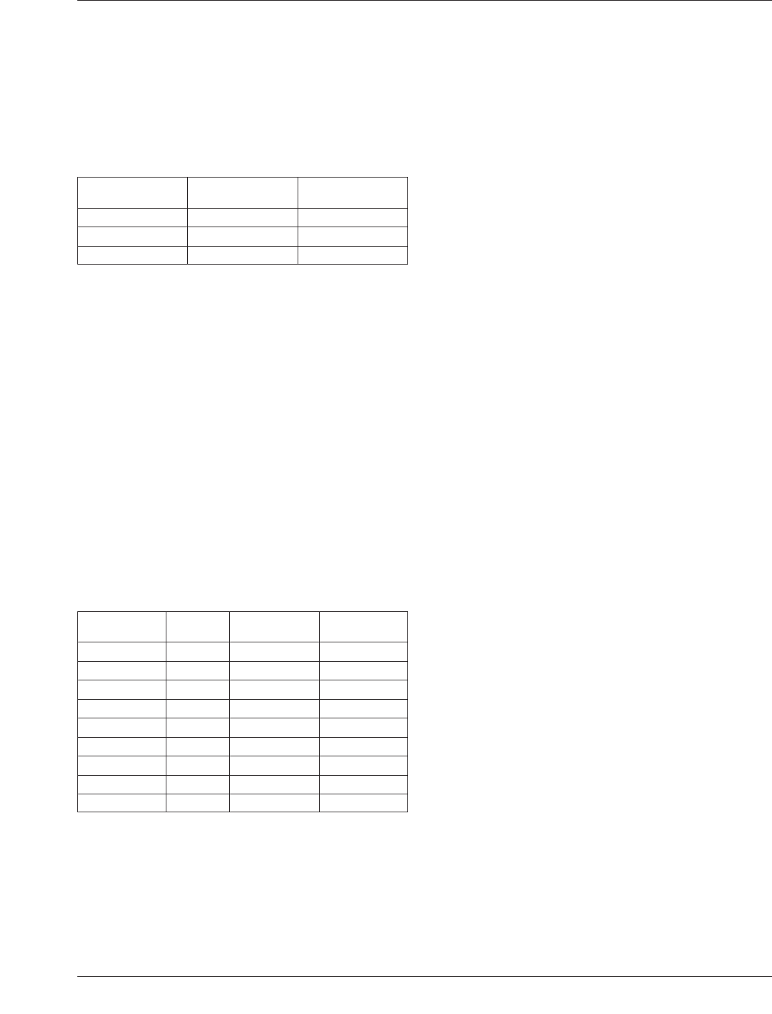
The information shown in Table 4-4 provides data on land
patterns and their variation to accommodate nine ball
diameters.
Many component manufacturers use solder mask-defined
lands (see 6.2.2). When this technique is employed, the
nominal land diameter should be increased by the amount
of solder mask encroachment on the land (usually about
0.1 mm). The opening in the solder mask window then
represents the diameter to which the ball will become
attached, while the actual land is slightly larger to accom-
modate the solder mask-defined land concepts. It should be
noted that routing density is decreased, since the land is
larger.
4.3.3 BGA Package Outline Body sizes for ball grid
arrays are divided up into the following two outline groups:
square and rectangular. The square outline package family
size ranges from as small as 4 mm x 4 mm and as large as
50 mm x 50 mm. In the fine pitch variations, the package
sizes increase in 1.0 mm increments. In the ranges above
21 mm x 21 mm, the body size increases in increments of
2.0 mm to 2.5 mm and the pitches are in the regular range.
Rarely will any of the fine pitch parts be found in sizes
larger than 21 mm x 21 mm. The rectangular BGA family
has the same size ranges from 4.0 mm to 50 mm but varies
by each application. This group can have many more varia-
tions than the square group. Rectangular sizes typically are
found to follow no fixed incremental progression. This
group is normally driven by the memory applications and
closely follows the die sizes. Rectangular sizes are nor-
mally standardized in small application specific families.
The fine pitch BGA components, equal to or less than 0.8
mm, rarely exceed 21 mm in body size.
A fine pitch ball grid array (FBGA) is a 0.50 to 0.80 mm
pitch solder balled array package that have fixed package
dimensions ‘‘D (Length)’’ and ‘‘E (Width).’’ The FBGA is
more like the plastic and ceramic BGA families described
above having fixed body dimensions. Although the FBGA
outline is typically only 20% larger than the die, it will not
change shape with every die shrink.
The die-size ball grid array package (DSBGA) is a 0.30 to
0.50 mm pitch solder balled array package that has variable
package dimensions ‘‘D (Length)’’ and ‘‘E (Width).’’ The
DSBGA package takes the shape of the die which normally
makes it a rectangular outline and is presently widely used
in Flash and DRAM Memory devices. The rectangular die
size (RDS) outline will likely change ‘‘D’’ and ‘‘E’’ dimen-
sions with every die shrink.
4.3.4 Ball Size Relationships The total variation of the
system considers three major issues: positioning, ball toler-
ance, and substrate tolerance. All three attributes added
together result in a worst case analysis; however, as with
other land patterns in the standard, a statistical average is
determined by using the RMS (root mean, square) value.
The trend toward higher pin-count ICs and smaller package
outlines has enabled companies to improve both product
functionality and performance. Table 4-5 will assist the
user in calculating variations in land pattern geometry for a
wide range of BGA applications, and shows the total varia-
tion in the system for each of the nine ball sizes identified
in the standards. As noted, the standard nominal dimension
for ball contact diameters are 0.15, 0.20, 0.25, 0.30, 0.40,
0.45, 0.50, 0.60, and 0.75 mm. Ball contact size for array
packages are influenced by the limit established for overall
package height, ball contact pitch and the desire to maxi-
mize solder joint reliability.
Table 4-3 Future Ball Size Diameters for DSPBGAs
Nominal Ball
Diameter (mm)
Tolerance
Variation (mm) Pitch (mm)
0.25 0.28 - 0.22 0.40
0.20 0.22 - 0.18 0.30
0.15 0.17 - 0.13 0.25
Table 4-4 Land Size Approximation
Nominal Ball
Diameter (mm) Reduction
Nominal Land
Diameter (mm)
Land
Variation (mm)
0.75 25% 0.55 0.60 - 0.50
0.60 25% 0.45 0.50 - 0.40
0.50 20% 0.40 0.45 - 0.35
0.45 20% 0.35 0.40 - 0.30
0.40 20% 0.30 0.35 - 0.25
0.30 20% 0.25 0.25 - 0.20
0.25 20% 0.20 0.20 - 0.17
0.20 15% 0.15 0.15 - 0.12
0.15 15% 0.10 0.10 - 0.08
January 2013 IPC-7095C
21
Copyright IPC-Association Connecting Electronics Industries
Provided by IHS under license with IPC
Not for Resale
No reproduction or networking permitted without license from IHS
--`,,```,,,,````-`-`,,`,,`,`,,`---