IPC-7095C-2013.pdf - 第68页
maximum conductor width recommendation for SMD sol- der lands; however, the maximum conductor width con- necting NSMD solder lands is 0.2 mm. Anything wider will have the ef fect of changing the solder land to an SMD typ…
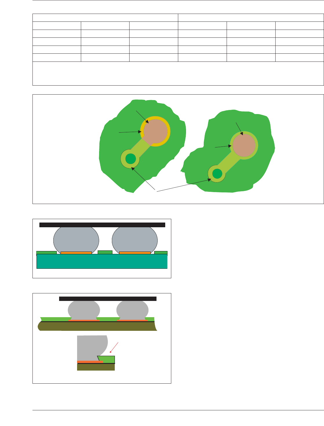
have a higher standoff. The effect is illustrated in Figure
6-5, which shows the contrast in joint geometry resulting
from solder mask defined lands (left side) and a metal
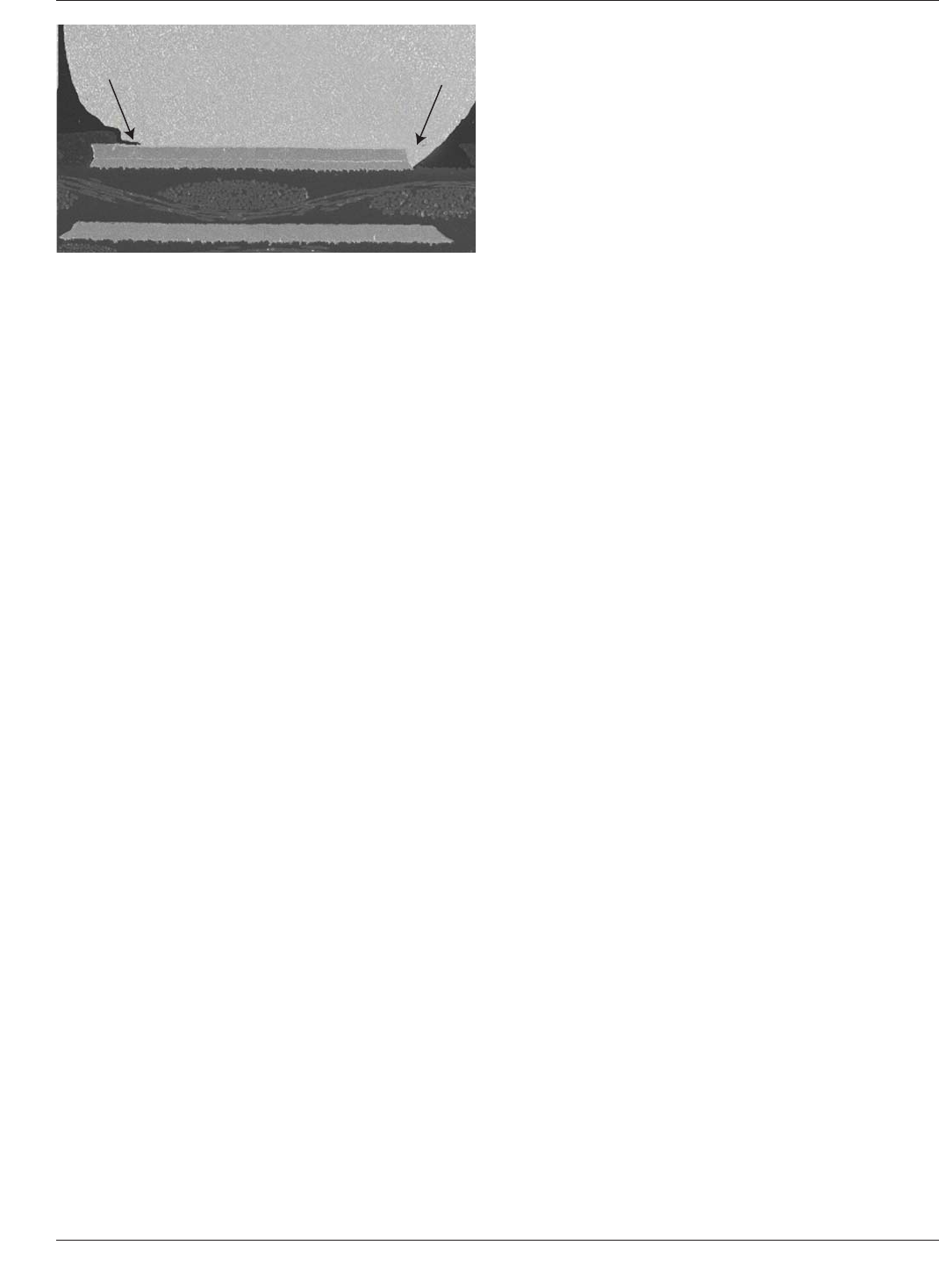
defined condition (right side). The stress concentration on
the solder mask defined land results in possible crack ini-
tiation at the mounting surface. The SMD lands adhere to
the board better because of the larger surface area of cop-
per and the overlapping solder mask. The major disadvan-
tage to SMD lands is the vulnerability of the solder joint at
the interface of solder mask and solder material. Some tests
indicate that the solder joint fatigue life has decreased sig-
nificantly when compared with nonsolder mask defined
(MD) lands. The major advantage is that this approach may
be used to prevent the land from pulling off of the board.
Land lifting, also known as cratering, usually occurs at the
corner balls. Because corner balls have a higher strain rate
and are more likely to fail, many times component manu-
facturers make these non-critical to function (CTF). In the
case of no CTF corner balls, it may be desirable to have
SMD lands in these locations.
6.2.3 Conductor Width The conductor width can affect
the routing of the BGA package. The wider the conductor,
the less room between lands for placing runs. There is no
Table 6-3 Maximum Solder Land to Pitch Relationship
Maximum Land Size
BGA Pitch Ball Size Standard Pad Via One Track Two Track
1.27 0.75 0.50 0.95 0.90 0.65
1.0 0.60 0.45 0.45 0.65 0.40
0.8 0.50 0.40 0.30 0.45 –
0.7 0.40 0.35 0.20 0.35 –
Assumption: 125/125 µm conductors and spaces
via land for 1.25 mm and 1.0 mm pitch BGA is 0.63 mm
via land for 0.8 mm and 0.7 mm pitch BGA is 0.5 mm
All values rounded down to 0.5 mm
IPC-7095c-6-2
Figure 6-2 Solder Lands for BGA Components
Copper Pad
Solder mask
away from pad
Via covered with solder mask for interconnection
Copper Pad
Solder mask
on pad
IPC-7095c-6-3
Figure 6-3 Metal Defined Land Attachment Profile
IPC-7095c-6-4
Figure 6-4 Solder Mask Stress Concentration
Solder Mask
Concentrates
Stress
Thermal Expansion
in “Z” Axis is Greater
for Solder Mask than
the Solder Ball
Cross Sectional
Area of Solder
Ball Reduced
January 2013 IPC-7095C
53
Copyright IPC-Association Connecting Electronics Industries
Provided by IHS under license with IPC
Not for Resale
No reproduction or networking permitted without license from IHS
--`,,```,,,,````-`-`,,`,,`,`,,`---
maximum conductor width recommendation for SMD sol-
der lands; however, the maximum conductor width con-
necting NSMD solder lands is 0.2 mm. Anything wider
will have the effect of changing the solder land to an SMD
type land at the location. For the same reasons, only one
conductor should be joined to any NSMD solder land. To
eliminate sharp corners, a fillet should be used where the
conductor connects to the solder land.
6.2.4 Via Size and Location Vias can be placed between
BGA solder lands on the land pattern. Via lands should be
kept small enough to provide clearance between them and
adjoining solder lands. The maximum via size that can be
used depends upon the size and type (SMD vs. MD) of
solder land used. However, it is recommended that the
smallest standard via land/drill size be utilized for the
board thickness. Vias with 0.6 mm lands and 0.35 mm
drilled holes are common for 1.5 mm and 1.27 mm pitch
BGAs, while 0.5 mm lands/0.25 mm drilled holes are used
for 1.0 mm and 0.75 mm pitch packages.
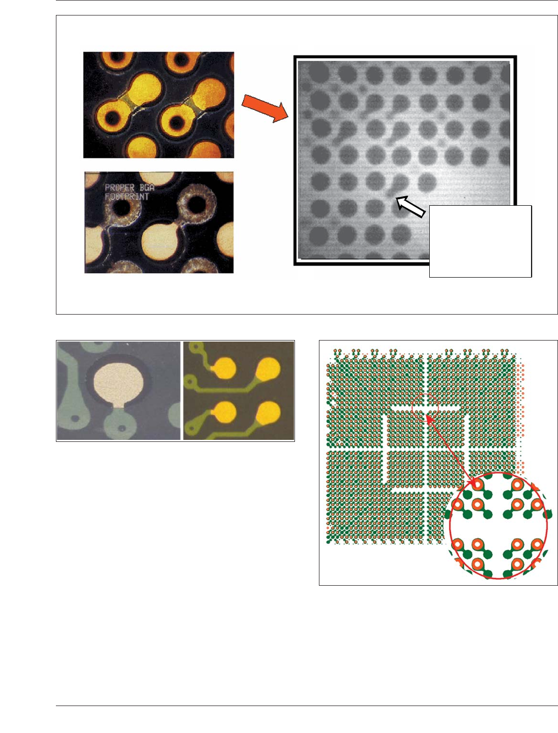
To minimize the risk of solder bridging between standard
sized vias and solder lands, vias can be either tented or
have solder mask encroaching (overlapping) the via land.
Covering the via lands will also reduce the risk of narrow
solder mask dams peeling off during BGA rework. See
Figure 6-6 for examples of covered vias and narrow solder
mask dams. Tented vias may not be reliable with some
combinations of solder mask and surface finish. The solder
mask opening on an encroached via should be just large
enough to allow flux and other contaminants to escape dur-
ing processing. Consult your board fabricator for capabili-
ties when planning to tent or use encroached solder mask
on vias. Also see Figure 6-7.
Other options for vias on BGA land patterns include blind
vias and microvias. Blind vias can be created using a stan-
dard drill process, laser ablation, or photo-defined through
wet or dry (plasma) chemistry. The outer and inner layers
are sequentially built and are then laminated together.
Because the via penetrates only the outer layers, a smaller
sized drill can be utilized. However, this option is generally
a large cost addition. Blind vias can be placed between sol-
der lands but, because of their smaller via lands, centering
the via between the solder lands is not as critical.
Microvias are created in a secondary operation and pen-
etrate the outer layers only. A standard microvia connects
layers 1 and 2 and/or n-1 and n. A typical microvia can
have a 0.3 mm land with a 0.1 mm hole size. Because of
this small size, the via can actually be placed in the center
of the solder land with the only noticeable effect being a
small dimple. The dimple can be avoided by using a Type
VII via protection concept in the design that fills and caps
the via. By placing vias directly in the land, the space
between BGA solder lands on the outer layers can be used
exclusively for routing.
One should establish a liaison with a board manufacturer
for options and rules before designing BGA land patterns
with blind or microvias.
6.3 Escape and Conductor Routing Strategies Unlike
peripherally leaded packages, BGA solder joints are not all
easily accessible on the top board layer. This is especially
true for BGA packages with large, full grid arrays. Addi-
tional layers may be required to route the signals out from
underneath the middle of these packages.
For example, a 1.27 mm pitch, 357-pin PBGA has a 19x19
full grid array without the corner solder balls. If 0.63 mm
solder lands are used, this leaves only 0.63 mm between
lands for routing conductors. This would permit only one
0.2 mm conductor between the lands, meaning that only
the outer two rows (136 pins total) of the package could be
routed out on the top layer. All other pins (221 total) would
need to join to vias and then be routed out through other
signal layers. If 125 µm conductors/spacing is used, two
conductors could be placed between lands so that the outer
three rows of pins (192 pins total) could be routed out on
the top layer, leaving the remaining pins (165 total) to be
routed using vias.
The via pattern for the board requires much tighter feature
control as the pitch for BGA, FBGA and CSP becomes
smaller.
Fanout patterns should show a distinctive cross for power.
There have been instances that power isolation has
occurred when the cross pattern was not used in BGA
fanout due to power clearances, creating a wall around the
internal power pins. The cross pattern also allows for an
area for internal or cross BGA nets to route. (see Figure
6-8).
Successful BGA fanout involves:
• Adherence to a placement grid in alignment with the
fanout grid whenever possible
• Protecting BGA fanout vias during routing
• Proper via and land sizes
Figure 6-5 Solder Joint Geometry Contrast
SMD geometry
with stress-
concentration
MD geometry
without stress-
concentration
IPC-7095C January 2013
54
Copyright IPC-Association Connecting Electronics Industries
Provided by IHS under license with IPC
Not for Resale
No reproduction or networking permitted without license from IHS
--`,,```,,,,````-`-`,,`,,`,`,,`---
An alternate method for BGA fanout is to not fanout the
perimeter pins in the outer two rows and columns of the
BGA. For the outer two rows, allow the router to drop the
‘‘fanout’’ via with a relaxed set of distance rules. The outer
two rows of relaxed fanouts create a dip-like pattern
around the BGA for the auto-router to complete. The space
between this dip pattern and the BGA pattern allow for
non-BGA nets to cross the area of the BGA without need-
ing to navigate the internal BGA fanout pattern. This
method can be tried when one is having problems routing
a board with BGAs.
To ease routing, power and ground pins can be placed in
the center of the array pattern so that they can be connected
directly to vias and not interfere with routing around the
outer edges of the package.
IPC-7095c-6-6
Figure 6-6 Good/Bad Solder Mask Design
Solder has been
sucked into via
due to improper
trace and solder
mask design.
BGA Trace and
Solder Mask Design
Showing Solder
Joint Impact
Solder has been
sucked into via
due to improper
trace and solder
mask design.
Solder has been
sucked into via
due to improper
trace and solder
mask design.
Figure 6-7 Examples of Metal-Defined Land
Figure 6-8 Quadrant Dog Bone BGA Pattern
January 2013 IPC-7095C
55
Copyright IPC-Association Connecting Electronics Industries
Provided by IHS under license with IPC
Not for Resale
No reproduction or networking permitted without license from IHS
--`,,```,,,,````-`-`,,`,,`,`,,`---