IPC-7095C-2013.pdf - 第87页
previous case, the printed circuit board supports the weight of the heat sink when the clips are actuated, but some stress can still be transferred on to the BGA solder balls during mechanical shock and vibration. In add…
6.7.4.4 Gels Gels are comprised of a lightly cross-linked
silicone polymer filled with metal or ceramic particles that
impart the thermal conductivity necessary for this TIM.
Gels combine the beneficial properties of greases and cured
adhesives, do not pump-out and do not require a post appli-
cation cure step. Their modulus is low enough to relieve
thermo-mechanical stresses and avoid interfacial delamina-
tions. They have high bulk thermal conductivities and have
been used in cooling BGA components containing high
wattage CPU devices.
6.7.4.5 Thermal Conductive Pressure Sensitive Tape
Thermal conductive pressure sensitive tape may occasion-
ally be used to impart the thermal conductivity necessary to
remove heat from the BGA. This thermal interface material
is becoming more widely used due to the ease of handling
and applying to the surfaces that are used for cooling BGA
components.
6.7.5 Heat Sink Attachment Methods for BGAs There
are quite a few techniques for attaching heat sinks to
BGAs. These are depicted in the following illustrations.
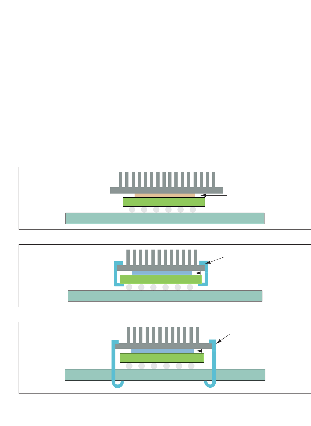
Figure 6-33 shows a heat sink attached to the top of a BGA
package with a thermally conductive adhesive. The adhe-
sive acts as both a thermal conduction medium as well as
a mechanical attachment medium. As mentioned above,
however, this technique requires a post solder thermal cure
step to cross-link the adhesive and harden it.
Figure 6-34 illustrates a heat sink attached to the top of a
BGA package with clips that hook on to a BGA substrate.
However, there is danger of damage to the solder joints
while attaching the clips. The thermal interface material in
this case is a grease, or PCM or gel, i.e., one that does not
provide a strong mechanical bond between the heat sink
and the top of the BGA package. This method has one
drawback. The weight of the heat sink is supported by the
package and, during mechanical shock and vibration, the
solder balls of the BGA have to bear the mechanical
stresses generated by the additional mass of the heat sink.
Figure 6-35 depicts the case of a heat sink attached to the
BGA with clips that hook into holes in the printed circuit
board. These holes do not have to be plated. Unlike the
IPC-7095c-6-33
Figure 6-33 Heat Sink Attached to a BGA with an Adhesive
BGA
Adhesive
Board
Heat Sink
IPC-7095c-6-34
Figure 6-34 Heat Sink Attached to a BGA with a Clip that Hooks onto the Component Substrate
Grease/
Gel/PCM
Board
Clip
BGA
Heat Sink
IPC-7095c-6-35
Figure 6-35 Heat Sink Attached to a BGA with a Clip that Hooks into a Through-Hole on the Printed Circuit Board
Board
Clip
Grease/
Gel/PCM
BGA
Heat Sink
IPC-7095C January 2013
72
Copyright IPC-Association Connecting Electronics Industries
Provided by IHS under license with IPC
Not for Resale
No reproduction or networking permitted without license from IHS
--`,,```,,,,````-`-`,,`,,`,`,,`---
previous case, the printed circuit board supports the weight
of the heat sink when the clips are actuated, but some stress
can still be transferred on to the BGA solder balls during
mechanical shock and vibration. In addition, the heat sink
may create a cantilevered load on the solder joint when the
assembly is in a vertical orientation. This load may lead to
premature solder joint failure.
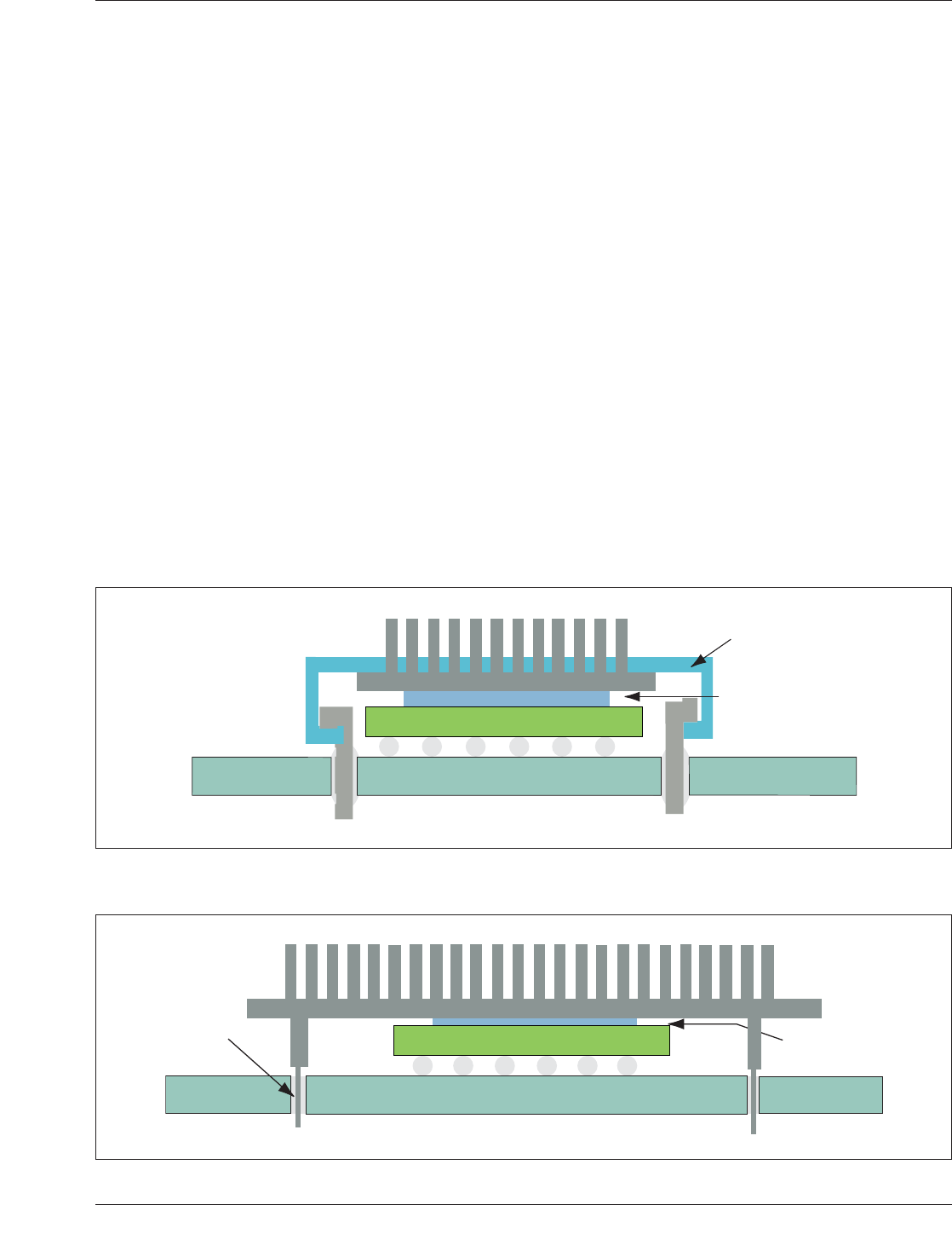
Figure 6-36 shows the case of a heat sink attached to a
BGA package with clips that hook on stakes that are wave
soldered into holes in the printed circuit board. This
method of attachment transfers even less stress on the BGA
solder balls during mechanical shock and vibration than the
previous case. However, the solder joints of the stakes will
bear most of this stress.
Figure 6-37 illustrates the attachment of the heat sink to a
BGA by directly soldering the heat sink into the board dur-
ing the wave soldering process step. The heat sink design
has four or more pins that insert into holes in the board
prior to the wave solder process. As opposed to the previ-
ous cases above, this method does not need any post
assembly processing to attach the heat sink.
The three methods in Figures 6-30, 6-31 and 6-32 have one
drawback not present in the first two. These methods
require holes in the printed circuit to be designed in. These
holes may reduce the trace routing real estate on all the
board layers. For highly dense board designs, this could
impact the final layer count of the board.
6.8 Documentation and Electronic Data Transfer The
documentation package for describing BGA components
usually consists of a master drawing, master pattern draw-
ing, copies of artwork (film or paper), mounting structure
assembly drawing, parts list, and schematic/logic diagram.
The documentation package may be provided in either hard
copy or electronic data. All information about documenta-
tion is also appropriate for electronic data transmission.
Since many CAD systems have their own native database,
everyone is promoting some form of unique format that has
a neutral concept, thus avoiding sending the native data-
base to the suppliers.
The lowest common denominator for years has been a
machine language. This may eventually be replaced by
such formats as the IPC-D-356, or IPC-2581. Archiving
electronic data should be in accordance with these docu-
ments. Delivery of computer generated data as a part of the
documentation package should meet the requirements
stated in those packages. With automated techniques, the
database shall detail all information that will be needed to
produce the printed board or mounting structure for the
bare die. This includes all notes, plating requirements,
IPC-7095c-6-36
Figure 6-36 Heat Sink Attached to a BGA with a Clip that Hooks onto a Stake Soldered in the Printed Circuit Board
Grease/
Gel/PCM
Board
BGA
Heat Sink
Clip
IPC-7095c-6-37
Figure 6-37 Heat Sink Attached to a BGA by Wave Soldering Its Pins in a Through-Hole in the Printed Circuit Board
Grease/
Gel/PCM
BGA
Heat
Sink
Pin
Board
January 2013 IPC-7095C
73
Copyright IPC-Association Connecting Electronics Industries
Provided by IHS under license with IPC
Not for Resale
No reproduction or networking permitted without license from IHS
--`,,```,,,,````-`-`,,`,,`,`,,`---

board thickness, etc. The test plots should be employed to
verify that the data matches the requirements.
Other documentation may include numerical control data
for drilling, routing, libraries, tests, artwork, and special
tooling. There are design and documentation features/
requirements that apply to the basic layout, the production
master (artwork), the mounting structure itself, and the end
item component or printed board assembly. All must be
taken into consideration during the design of the mounting
structures for the bare die, or the mounting structure for the
BGA. Documentation shall meet the requirements of IPC-
2611. In order to provide the best documentation package
possible, it is important to review IPC-2611 and identify all
the criteria that are affected by the design process.
6.8.1 Drawing Requirements During the formal design
review prior to layout, special tools that can be generated
by the design area in the form of artwork or numerical
control data shall be considered. This tooling may be
needed by fabrication, assembly, or testing. Examples of
such tooling are drilling data files, solder paste stencils,
data for component placement, ICT fixture data, and art-
work in the form of layered graphics, silk screen and sol-
der mask.
When viewing the documentation, it is always viewed from
the primary side. All phototool generation is viewed from
that same direction. The definition of layers of the product
shall be viewed looking through the particular part from
the primary side.
Accuracy and skill must be sufficient to eliminate misinter-
pretation during the artwork generation process. This
requirement can be minimized by adhering to a grid or
pitch of the component terminations, which drive so many
features on the board or the bare die.
Layout notes should be as complete as possible with the
addition of appropriate notations. Marking requirements
and revision status level definition are key to maintaining
configuration management conditions. It is especially
important for the engineering review cycle, a quoting
effort, and when the document is used by someone other
than the originator.
6.8.2 Equipment Messaging Protocols Throughout the
electronics industry manufacturing consists of numerous
steps, each of which often centers around one supplier’s
equipment. Although the steps are generally well-
automated within themselves, they are only peripherally
connected to one another. Proprietary data formats and
communications protocols prevent the islands of automa-
tion from talking to one another. This condition also pre-
vents factory managers from monitoring, understanding,
and possibly correcting the manufacturing process to
improve throughput and product quality.
In the last few years, building on an International Electron-
ics Manufacturing Initiative (iNEMI) funded project, the
IPC has standardized data syntax and semantics in elec-
tronics assembly, establishing rules for data exchange both
on a single factory floor and between that floor and the rest
of a manufacturing organization. The results have been
published as the IPC CAMX (computer-aided manufactur-
ing using the extensible markup language [XML]) stan-
dards: The standards are:
• IPC-2541, Generic Requirements for Electronics Manu-
facturing Shop-Floor Equipment Communication
• IPC-2546, Sectional Requirements for Shop-Floor Equip-
ment Communication Messages (CAMX) for Printed Cir-
cuit Board Assembly
• IPC-2547, Sectional Requirements for Shop Floor Equip-
ment Communication Messages (CAMX) for Printed Cir-
cuit Board Test, Inspection and Rework
At the heart of the standard is a framework with an inter-
mediary. This is the ‘‘message broker’’ that handles infor-
mation exchange and complies with the IPC-2501 Standard
(‘‘Definition for Web-based Exchange of XML Data’’). The
message broker can be thought of as a post office or a mail
server. Messages are sent to the server and, when the infor-
mation is needed, it is asked for by the equipment or the
manager who wants the data.
In a factory, several lines of equipment and several appli-
cations may connect to the message broker at the same
time. Individual elements need not know any details about
the nature, configuration, or format of the others. They
communicate directly only with the broker. When people
and equipment need specific information, the broker pro-
vides it in the correct format.
6.8.2.1 Implementation It is relatively easy to set up the
infrastructure and web-based tools to monitor several sets
of manufacturing equipment, including in-circuit testers,
and several suppliers’ pick-and-place machines. The setup
can be used to gathered performance and functional feed-
back data on the message broker. The message broker can
usually be up and running in two days, being able to con-
nect reasonably easily with both legacy equipment and any
XML-ready equipment using an infrastructure that is in
place at the manufacturing site. In a careful installation, it
is also possible to avoid compromising network security
requirements.
Using internet standards like HTTP and XML ensures the
interoperability between different platforms. Although an
application has never been run against a running message
broker before, it can be adapted to the existing communi-
cation framework on site. One important goal of the IPC-
CAMX standards is to lower the technological barrier to
ease the integration of sophisticated equipment like pick-
and-place machines and test equipment, as well as simpler
equipment like printed board handlers. The CAMX stan-
dards provide data about the products under manufacture,
IPC-7095C January 2013
74
Copyright IPC-Association Connecting Electronics Industries
Provided by IHS under license with IPC
Not for Resale
No reproduction or networking permitted without license from IHS
--`,,```,,,,````-`-`,,`,,`,`,,`---