IPC-7095C-2013.pdf - 第64页
6 PRINTED CIRCUIT ASSEMBLY DESIGN CONSIDER- ATION 6.1 Component Placement and Clearances It is recom- mended that suf f icient clearance (3 mm to 5 mm) be pro- vided around BGAs to facilitate rework. The high-end clearan…
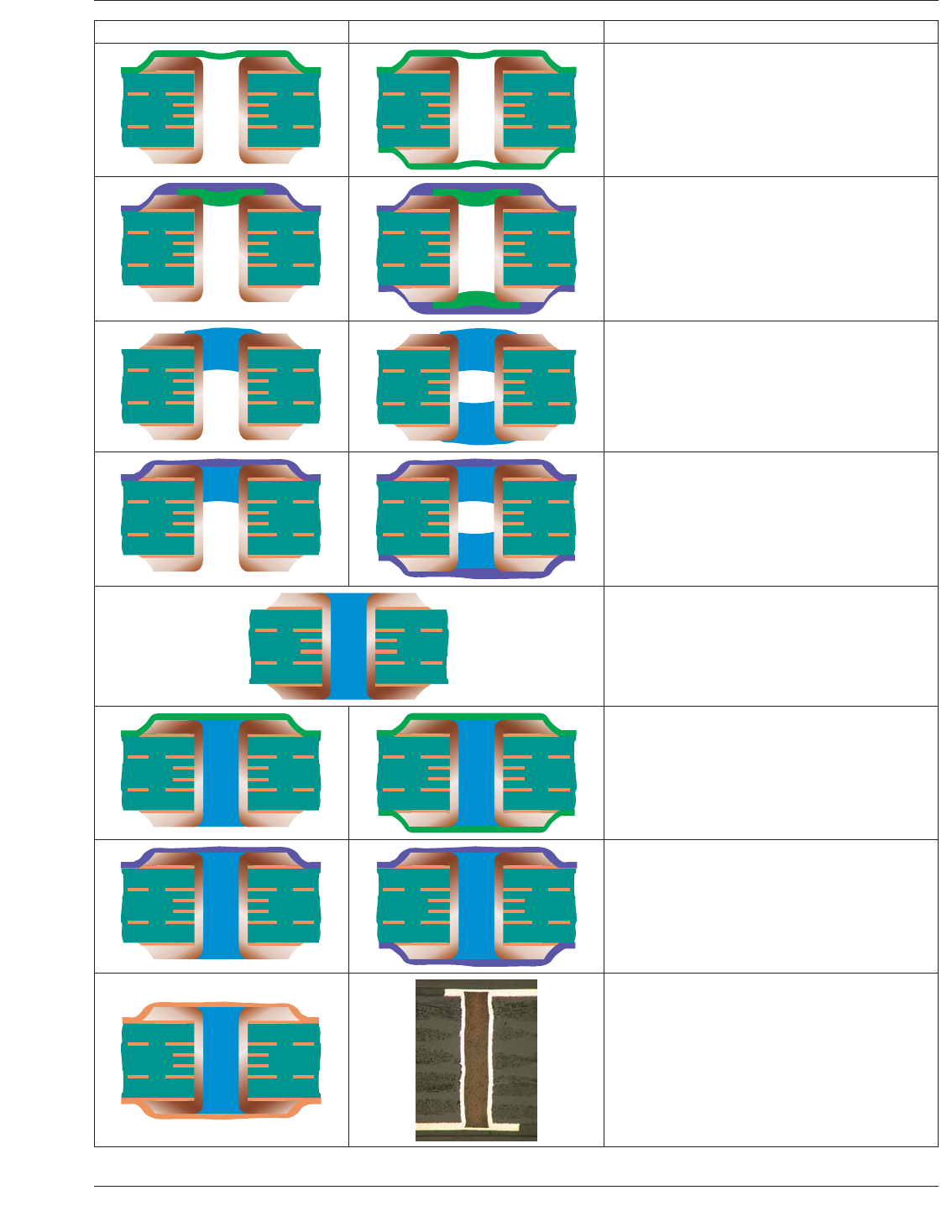
One side Type a Two sides Type b
Tented Via (Type I Via)
A via with a dry film mask material applied
bridging over the via wherein no additional
materials are in the hole. It may be applied
to one side.
(Type I-a) or both sides (Type I-b) of the via
structure (IPC-4761, Figure 5-1).
Tented and Covered Via (Type II Via)
A Type I via with a secondary covering of mask
material applied over the tented via. The material
may be applied to one side (Type II-a) or both
sides (Type II-b) of the via structure (IPC-4761,
Figure 5-2).
Plugged Via (Type III Via)
A via with material applied allowing partial
penetration into the via. The plug material
may be applied from either one side (Type III-a)
or both sides (Type III-b) of the via structure
(IPC-4761, Figure 5-3).
Plugged and Covered Via (Type IV Via)
A Type III via with a secondary covering of
material applied over the via. The plug and
secondary covering material may be applied
from either one side (Type IV-a) or both sides
(Type IV-b) of the via structure (IPC-4761,
Figure 5-4).
Filled Via (Type V Via)
A via with material applied into the via targeting
a full penetration and encapsulation of the hole
(IPC-4761, Figure 5-5).
Filled and Covered Via (Type VI Via)
A Type V via with a secondary covering of
material (liquid or dry film soldermask) applied
over the via. The covering material may be
applied from either one side (Type VI-a) or
both sides (Type VI-b) of the via structure
(IPC-4761, Figure 5-6).
Filled and Capped Via (Type VII Via)
A Type V via with a secondary metallized
coating covering the via. The metallization
is on both sides (IPC-4761, Figure 5-7).
Partially Filled Via
The illustrations show a via filled with
nonconductive epoxy and then plated
over with copper. This is commonly
used for via in pad applications
(IPC-4761, Figure 5-8).
Figure 5-12 Via Plug Methods
January 2013 IPC-7095C
49
Copyright IPC-Association Connecting Electronics Industries
Provided by IHS under license with IPC
Not for Resale
No reproduction or networking permitted without license from IHS
--`,,```,,,,````-`-`,,`,,`,`,,`---
6 PRINTED CIRCUIT ASSEMBLY DESIGN CONSIDER-
ATION
6.1 Component Placement and Clearances
It is recom-
mended that sufficient clearance (3 mm to 5 mm) be pro-
vided around BGAs to facilitate rework. The high-end
clearances are recommended, especially for CBGA when
using a step stencil to deposit solder paste and using hot air
for rework. However, if using diode laser systems for
rework the spacing can be reduced to 0.5 mm to 1.0 mm
since laser rework does not impact adjacent components.
6.1.1 Pick and Place Requirements An advantage of
BGA packages over other advanced, high-pin count pack-
ages (fine pitch, TAB, PGA, etc.) is the ability to be placed
using existing surface mount placement equipment. BGAs
are more forgiving in the pick-and-place process because
they self-align.
6.1.2 Repair/Rework Requirements Repair/rework of
BGA components is a major driver for component spacing
requirements. A typical BGA rework method requires five
steps:
1) heating the solder joints to reflow temperatures for
package removal;
2) removal and clean-up of solder on the BGA land pat-
tern;
3) application of new solder paste or flux;
4) placement of the new BGA package;
5) heating the solder joints to reflow temperatures for
assembly of the BGA component to the circuit board.
A keepout area may be needed for each of these steps.
Rework equipment manufacturers can provide specific
details regarding necessary keepout areas. General rules are
outlined below.
Table 5-4 Via Fill Options
Top Bottom Top & Bottom No Plug
Pros
Increase rework robustness Yes Yes Yes No
Reduce secondary reflow risk at wave Yes Yes Yes No
Prevent solder drain Yes Yes Yes No
Cons
Secondary Fab process Yes Yes Yes No
Component side height profile restriction
less than 50 µm
above solder mask
No
less than 50 µm
above solder mask
No
Flux contaminant concern
Yes – (if exposed to
wave solder directly)
No No No
Plug integrity concern
Yes (tented, plugged)
No (filled)
Yes (tented,
plugged)
No (filled)
Yes (tented, plugged)
No (filled)
No
IPC-7095c-5-13
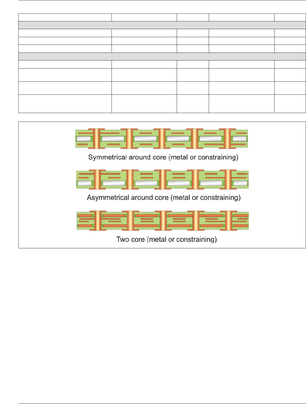
Figure 5-13 Metal Core Board Construction Examples
IPC-7095C January 2013
50
Copyright IPC-Association Connecting Electronics Industries
Provided by IHS under license with IPC
Not for Resale
No reproduction or networking permitted without license from IHS
--`,,```,,,,````-`-`,,`,,`,`,,`---

Nearly all hot air methods use a nozzle system that fits
down over and/or around the BGA package to heat the sol-
der joints for removal and reflow. A component keepout
area of 2.5 mm away from the outer edge of the oven
nozzle is suggested. Including the nozzle size results in a
3.8 mm clearance from the component body. This spacing
around the BGA provides room for the nozzle and reduces
the risk of heating solder joints of adjacent components
above the reflow temperature. When using laser for rework,
the keepout area can be reduced to under 1 mm.
After a BGA package has been removed from the board
during repair, the solder lands must be cleaned and new
solder paste or flux applied before a new component can be
placed. If the solder paste or flux is dispensed using manual
methods, or if solder paste is applied using an automated
dispensing system, then there are no special component
keepout areas required. However, many repair systems use
a miniaturized stencil and squeegee to manually apply sol-
der paste either to the lands on the board or onto the balls
of the component. In general, a minimum of 3 mm compo-
nent keepout (i.e., the nominal distance between the body
of the component and the body of the neighboring compo-
nent) is needed so that both the nozzle clearance require-
ment and the mini-stencil requirement can be met when
printing to the lands on the board. The existence of a high
profile neighboring component may require the minimum
distance to be much larger than the stated minimum value.
6.1.3 Global Placement There are no special global
placement requirements for BGA packages. However, it is
recommended that they not be placed near the board cen-
terlines. This reduces the potential of coplanarity problems
associated with the board warping during reflow. In addi-
tion, BGA packages should not be placed next to large
through-hole components, as these can stiffen the board
and significantly increase localized BGA corner joint
stresses. In some cases, one might want to take advantage
of certain features that might actually help protect the BGA
if the induced strain relative to the BGA corners are
reduced by the stiffness caused by nearby through-hole or
other components. Finally, BGA packages should not be
placed with their diagonals in line with mounting stand-off,
bosses, and screws that support or secure the printed board
assembly, since this can induce levels of stress on the cor-
ner balls, which are more susceptible to damage.
6.1.4 Alignment Legends (Silkscreen, Copper Features,
Pin 1 Identifier)
Alignment features printed on the circuit
board are recommended for BGA packages to verify com-
ponent alignment before and after reflow. BGA packages,
especially PBGA, will self-align during reflow, even when
placed up to 50% off the lands. As a result, any misalign-
ments are generally one land diameter length or more off.
Alignment features will help verify that the component
placement is sufficiently accurate with visual inspection.
Silkscreen and copper are the two main materials used for
alignment legends. Silkscreen is the most visible material,
but requires the additional process step during board manu-
facturing. Copper alignment legends are created at the
same time all other copper features are created and, there-
fore, lead to more accurate placement. Higher speed cir-
cuitry may be affected by the ungrounded copper in this
solution. Unconnected copper conductors can collect a
capacitance which will dissipate uncontrollably.
In many instances, legends are used by equipment or indi-
viduals to evaluate the alignment of the BGA during the
placement operation. For peripheral leaded components,
the fiducial has been standardized so that placement equip-
ment can adjust the movement of the placement head
accordingly and improve the final component positioning.
Local fiducials are often placed at opposite corners to allow
adjustment for the theta angle. This technique has been
incorporated into many placement tools and equipment.
The use of fiducials may not provide the most obvious
condition for human inspection; however, most inspectors
can approximate that the package is properly centered
between two fiducials in order to verify their position. In
some instances, companies have used angle brackets in
place of the fiducials to assist the human eye in making this
judgment; however, the camera for placement equipment is
not familiar with that configuration, thus the practice is not
the most conducive for automatic assembly (see Figure
6-1).
Using silkscreen, the entire package can be outlined for
easy visual alignment. Another alignment pattern com-
monly used is to mark just the corners of the BGA pack-
age. Corner marks should only be 0.8 mm long on each
side. Copper can be used for corner marks, since it won’t
interfere with routing runs, as long as it does not affect cir-
cuitry performance such as unwanted capacitance.
All alignment legends should be offset 0.25 mm away from
the outer edge of the BGA package. This gives sufficient
clearance to view the features all around the BGA package.
Pin 1 identifiers are required on BGA land patterns. This
identifier can be a caret, dot, or other easily visible shape.
The Pin 1 identifier can be either silkscreen or copper and
IPC-7095c-6-1
Figure 6-1 BGA Alignment Marks
January 2013 IPC-7095C
51
Copyright IPC-Association Connecting Electronics Industries
Provided by IHS under license with IPC
Not for Resale
No reproduction or networking permitted without license from IHS
--`,,```,,,,````-`-`,,`,,`,`,,`---