IPC-7095C-2013.pdf - 第123页
not significant at the larger ball image sizes but becomes more important when the land diameter shrinks to accom- modate a smaller ball or smaller BGA pitch. This is shown through the determination of the area connected …
much higher than that of solder joints after 1X reflow. For
example, the mean value of %voiding in solder joints after
3X reflow is about two times the %voiding level in solder
joints after 1X reflow. This is because the multiple reflow
cycles give extra time for existing voids to grow and
expand, or for small voids to coalesce together to form
bigger voids, when the solder joints are molten. This
growth and coalescence mechanisms have been confirmed
through analysis of 3D CT X-ray images before and after
each SMT reflow cycle.
7.7.1.7 Land Surface Finish The impact of land finish
type on process voiding is still not clear. But co-deposited
volatile organic compounds from surface finish plating
operations is believed to generate more process voids in
BGA solder joints. Although there has been much debate
on the impact of different land finishes, the voiding level of
these different finishes does not vary too much.
BGA voiding has become a focus in electronic industry due
to quality concern. For quality issue, some SMT process
parameters are essential to the voiding level in the BGA
solder joints. For example, if the component is exposed to
high humidity conditions or elevated temperatures, the sol-
der balls will have a layer of oxide crust, which could lead
to more voiding trapped in solder joints in reflow soldering
process. The other SMT process parameters which can sig-
nificantly impact voiding levels include multiple reflow
and solder paste formulation. Inspection of voiding levels
of BGA components is very important in order to under-
stand the percent, size and location of voids caused by the
SMT process.
There is no data showing a relationship between the BGA
void and reliability. Size of BGA voids is insufficient to
define acceptance criterion for fatigue life of the solder
joints. Macro process voids observed in X-ray images may
not cause any significant reliability impact, but microvoids
which cannot be seen in X-ray images may deleteriously
impact reliability. Large voids away from the solder joint to
component land interface do not impair the solder joint
fatigue life, but small voids at the interfaces can be
‘‘zipped’’ through once a crack starts. Location of voids
within the solder joint is as much, if not more, important
than void size.
7.7.2 Process Control Criteria for Voids in Solder
Balls
There is a continuing need for process development
and control to accommodate changing technologies. As
BGA land sizes, solder ball sizes and land pitch continue to
decrease, the dimensional parameters used on the produc-
tion floor need to change. New materials and processes
may be required to meet quality and reliability goals.
Voids will likely be encountered during various stages of
product life from development through manufacturing.
Maintaining a minimum acceptable standard is necessary to
assure that the product meets customer expectations,
product-life and reliability requirements. Manufacturers
need to use process control and continuous product
improvement techniques for void control. Readily available
statistical process control and process improvement tools
may be used.
A change in frequency and size of voids should indicate a
need for process control as well as improving the process
and materials. A baseline can be used to determine the need
for process adjustments to control the frequency and size of
voids. In addition, a void size limit could be established.
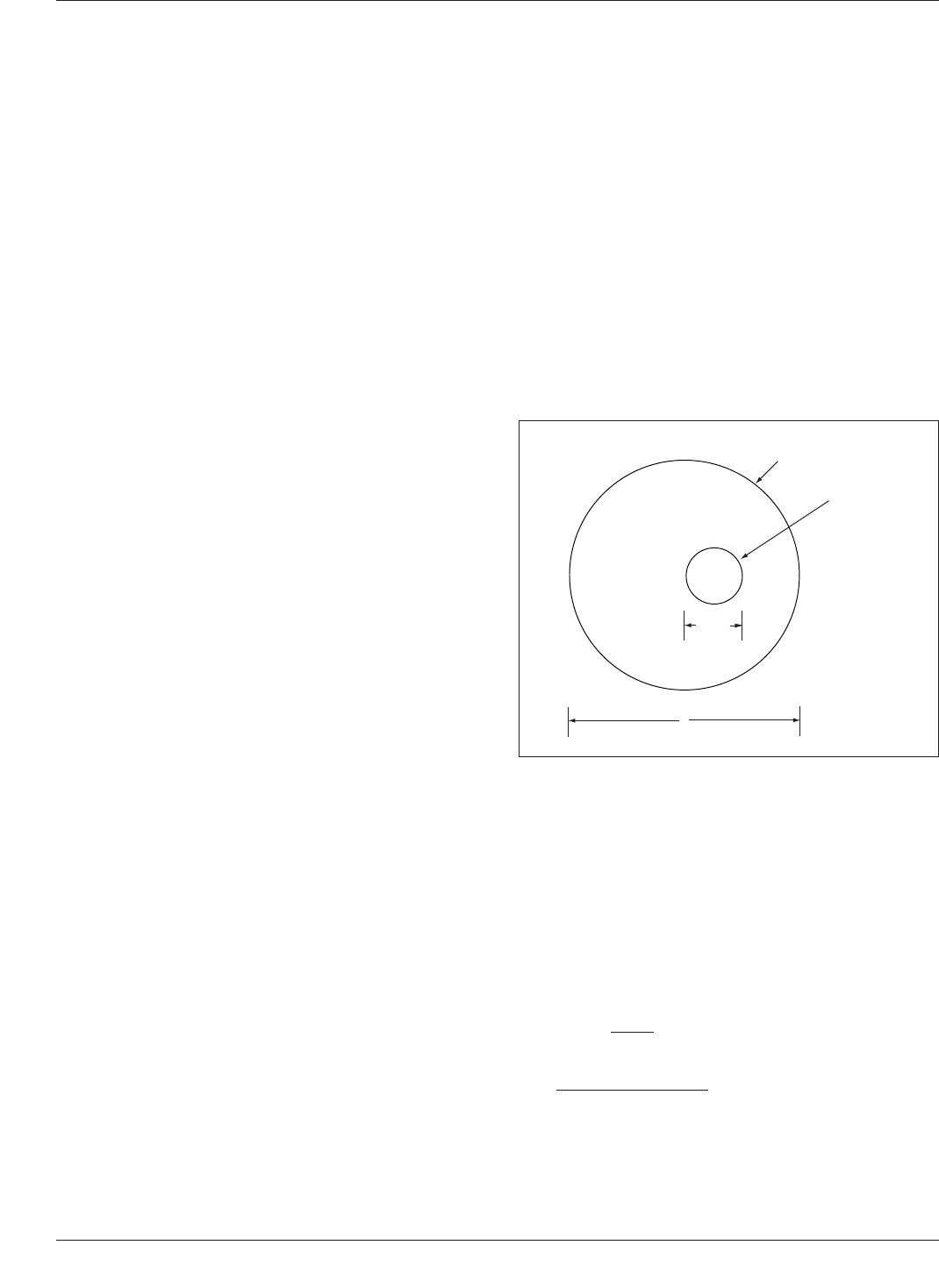
Size is determined in relationship to the ball. Thus a void
size larger than 25% of the solder ball’s cross-sectional
image diameter is approximately 6% of the total projected
area variation (see Figure 7-46). Any such process control
limits should be set with customer agreed-to contractual
commitment.
When there is more than one void per solder ball, the
dimensions of the voids will be added to calculate the total
voiding in that solder ball.
The equations for determining percentages are as follows
and all relate to the diameter of the ball or the contact sur-
face.
Void diameter percentage
Dvoid
Dball
x 100 = void percentage
Void Area
Contact or Ball Area
x 100 = void percentage
* Area is determined using the diameter and Pi (πr
2
).
Once the relationship of the void diameter to the ball image
diameter is known, the actual numbers and size relation-
ships become important. A 25% difference in diameters is
IPC-7095c-7-46
Figure 7-46 Example of Voided Area at Land and Board
Interface
Solder Outline
Void Outline
0.25 d
d
IPC-7095C January 2013
108
Copyright IPC-Association Connecting Electronics Industries
Provided by IHS under license with IPC
Not for Resale
No reproduction or networking permitted without license from IHS
--`,,```,,,,````-`-`,,`,,`,`,,`---

not significant at the larger ball image sizes but becomes
more important when the land diameter shrinks to accom-
modate a smaller ball or smaller BGA pitch. This is shown
through the determination of the area connected to the land
after the void has been determined.
Image of a BGA ball 600 µm with a 25% void =
(Dvoid)
2
= 22500 µm
2
(Dball)
2
= 360000 µm
2
= 6.25% area taken up by the void.
Comparing area of ball image with area of void image
leaves 265073 µm
2
remaining (πr
2
).
Image of a BGA ball 300 µm with a 25% void =
(Dvoid)
2
= 5625 µm
2
(Dball)
2
= 90000 µm
2
= 6.25% area taken up by the void.
Comparing area of ball image with area of void image
leaves 66268 µm
2
remaining (πr
2
).
Appendix A provides recommendations for process
improvement regarding the occurrence of voids in the ball
at incoming (Type A and B voids) as well as those voids
that are discovered after the assembly has gone through the
attachment processes (Type C, D and E voids).
See Appendix A, Table A-1 to Table A-3 for corrective
action indicators.
7.7.3 Process Control Criteria The accept/reject criteria
for BGA assemblies is established by J-STD-001 and IPC-
A-610. Those documents provide the final accept/reject cri-
teria used in contractual agreements. The process correc-
tive actions identified in the following sections are intended
to establish continuous process improvement based on the
size of the voids, their location, and method of determina-
tion of the void occurrences.
Void clarification is also defined as to whether the voids
occur prior to attachment to the mounting structure, or after
the assembly has taken place. This useful information can
be correlated to reliability conditions based on the end-use
environment. Using the size limitation structure a process
can be established that helps to meet the customers’ defined
acceptability conditions (see Appendix A).
7.8 Solder Defects
7.8.1 Solder Bridging
Solder bridging is unacceptable.
Electrical testing, optical inspection (endoscope) or X-ray
inspection is necessary to detect solder bridging. Poor sol-
der paste printing, inaccurate placement, manual ‘‘tweak-
ing’’ after placement, and solder splattering during reflow
are typical causes of solder bridging. Solder balls too large
for the gap between the two substrates can also cause
bridging.
7.8.2 Cold Solder The reflow profile should reach tem-
peratures high enough to ensure that the solder melts com-
pletely and proper wetting of the land surface occurs. A
cold solder joint can reduce mechanical integrity and can
cause it to fail electrically or function intermittently. Opti-
cal inspection after cross-sectioning is the best way to
inspect for cold solder joints.
7.8.3 Opens Solder opens are also unacceptable. Electri-
cal testing, optical inspection (endoscope) or X-ray inspec-
tion is necessary to detect solder opens. Poor solder paste
printing, inaccurate placement and manual ‘tweaking’’ after
placement are typical assembly-related causes of solder
opens. Coplanarity and substrate solderability problems can
also cause opens. Excessive mechanical stress can also
cause solder joints to crack and create opens.
7.8.4 Insufficient/Uneven Heating A common process
problem is insufficient or uneven heating of the BGA. This
problem occurs more often during rework but can also be
seen in production when working with multilayer boards
with many ground or power planes. The problem can also
occur on double-sided boards when a shielded component
is on the backside near the location of the BGA. The prob-
lem results when a thermal conductor removes the heat
from the BGA before complete reflow can occur. The
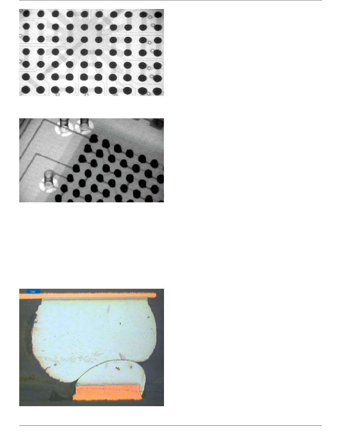
X-ray image of this problem is characterized by a variation
in the size of the solder balls at different locations under
the package.
Insufficient heating is generally characterized in an X-ray
image by small partially reflowed solder balls in the center
or to one side of the package. Insufficient heating may also
be characterized by a jaggedness around the perimeter of
these solder balls; indicating that the solder partially
reflowed but not long enough to completely wet to the land
and collapse to a nice round ball. Misalignment of the sol-
der ball with respect to the land is also an indicator of
inadequate heating. The X-ray image of misalignment is
characterized by elongated solder balls which may or may
not have a consistent orientation.
X-ray inspection at a 45° angle is also a useful technique
to locate signatures associated with insufficient heating or
nonwetting. The solder ball should contact and completely
wet to the land forming a smooth pillar. Signatures associ-
ated with insufficient heating include incomplete wetting to
the land, or an image elongation in the solder connection
indicating that the solder ball and solder paste did not flow
together to form a single solder joint (see Figures 7-47 and
7-48).
January 2013 IPC-7095C
109
Copyright IPC-Association Connecting Electronics Industries
Provided by IHS under license with IPC
Not for Resale
No reproduction or networking permitted without license from IHS
--`,,```,,,,````-`-`,,`,,`,`,,`---
7.8.5 Head-on-Pillow BGA head-on-pillow (HoP) solder
joint is defined as a joint that is comprised of two metallur-
gical distinct masses. One formed from the BGA ball and
the other from the reflowed solder paste. They have incom-
plete or no coalescence. This defect is known by many
other names such as head and pillow, head in pillow, ball
in cup, ball in socket, and hidden pillow (see Figure 7-49).
The sequence of Head-on-Pillow defect formation is
explained in Figure 7-50. First, the BGA ball is placed on
the solder paste which has been printed on the printed cir-
cuit board (PCB) lands (Figure 7-50 (a)). As the BGA on
the PCB enters the reflow soldering oven and its tempera-
ture increases, a gap develops between the ball and the sol-
der paste due to some factor, such as dynamic warpage of
the package and/or PCB (Figure 7-50 (b)). The solder on
the PCB land melts and flux covers its surface. The solder
ball also melts and its surface, which typically has little or
no flux covering it, starts to oxidize (Figure 7-50 (c)),
When the BGA package collapses, the ball once again
makes contact with the molten solder paste mass. At this
time, if the ball and the molten solder paste mass coalesce
together, then a good solder joint is formed. But, if there is
insufficient flux activity and too much oxide coating on the
surface of the ball, it results in head-on-pillow.
7.8.5.1 Dynamic Warpage If the package warps during
reflow due to Coefficient of Thermal Expansion (CTE)
mismatch between the substrate and silicon as the package
temperature rises in the oven, the warping effect will cause
some solder balls to be lifted up from the solder paste on
the board. This action increases the oxide growth on the
surface of the ball as flux is left behind on the pad, leaving
the ball devoid of flux. Usually when package warpage is a
primary cause, the HoP defect will occur at the highest
warpage area of the package and adjacent joints will be
elongated. Figure 7-51 shows a high warpage BGA were
the corners are lifted resulting in HoP.
Boards may warp or sag during reflow resulting in
increased gap between the paste and the balls on the pack-
age. When the board is too thin and not supported during
reflow, board warpage can be a primary cause for HoP.
Usually when either board or package warpage is a primary
cause, more than one ball will show sign of HoP defect.
Also the adjacent joints will be elongated.
7.8.5.2 Reflow profile The reflow profile parameters
have strong impact on HoP because of temperature differ-
ential (dT). The dT can be seen within a single component
due to board design (copper distribution), laminate or pack-
age material, and the type and size of the package. There is
also dT between the outer and inner rows of BGA balls
because of airflow.
Generally, the temperature of the outer row of BGA balls
are higher than the temperature of inner row balls, result-
ing in time delay between outer and inner row balls melt-
ing. However, even though they melt at different times, the
package collapses only after the inner ball melt. This time
delay also exposes the outer two balls to high temperatures
for longer time without the protection of flux. This results
in their oxidation and, hence, contributes to HoP. This time
difference between inner and outer ball becoming liquidus
Figure 7-47 X-Ray Image Showing Uneven Heating
Note the solder balls are larger at the bottom than the top.
Figure 7-48 X-Ray Image at 45° Showing Insufficient Heat-
ing in One Corner of the BGA
Note the irregular shape of the solder bonds at the top of the image.
Figure 7-49 Example of Head-on-Pillow Showing Ball and
Solder Paste have not Coalesced
IPC-7095C January 2013
110
Copyright IPC-Association Connecting Electronics Industries
Provided by IHS under license with IPC
Not for Resale
No reproduction or networking permitted without license from IHS
--`,,```,,,,````-`-`,,`,,`,`,,`---