IPC-7095C-2013.pdf - 第170页
ANSI/IPC-T -50 T erms and Definitions for Interconnecting and Packaging Electronic Circuits Definition Submission/Approval Sheet The purpose of this form is to keep current with terms routinely used in the industry and the…
A.1 Process Characterization The process characteriza-
tion information is based on void size and follows the rec-
ommendations of the flow diagram shown in Figure A-1.
The combination of void location, void size, and number of
occurrences helps to establish the actions required based on
the standard IPC three class structures. Table A-1 identifies
the recommendations for ball pitches of 1.5, 1.27 and
1.0 mm. Table A-2 identifies the recommendations for ball
pitches of 0.8, 0.65, 0.5 mm. Table A-3 identifies the rec-
ommendations for pitches of 0.5, 0.4 and 0.3 mm using the
via-in-pad technology.
All three tables identify the particular void types and relate
this information to the number of occurrences that there
could be in the three performance classes adopted by IPC.
The evaluation of an increase in the number of voids that
has been set as a target value can be a good aide to deter-
mining a process shift or a required change in some of the
process parameters. A process change should be driven by
an appropriate SPC methodology which should be used
during normal production cycles.
The use of these tables should also be for new product
introduction, product and process qualifications, equipment
set changes, component qualifications, response to cus-
tomer feedback and any similar change to the process or
parameters. The sampling plan used should be done at a
printed circuit assembly level, unless the SPC results show
a component related issue i.e., voids in one collapsible
BGA and no voids across the other collapsible BGAs on
the board. In this case, the sampling plan should be
executed at a component level of the suspect component
part rather than examining the assembly process.
Fine Pitch BGAs – The amount of attachment area that
remains after the void is identified in the fine pitch BGAs
is much less than in the standard pitch BGA. Table A-2 is
intended to show the corrective actions that should be
taken when the X-ray image shows the presence of voiding
in the incoming evaluation of the component or the evalu-
ation after assembly. The ball image is based on the BGA
pitch and, as it gets smaller, so does the land and the resul-
tant attachment area. The recommendations for corrective
action have taken this into account and reduced the void
size to compensate and thus improve the final attachment
reliability.
Via-in-Pad Design in Fine Pitch BGAs – As designs get
into finer and finer pitch, the need to obtain sufficient rout-
ing space encourages the use of microvias and via-in-pad
design. The conditions become more critical especially in
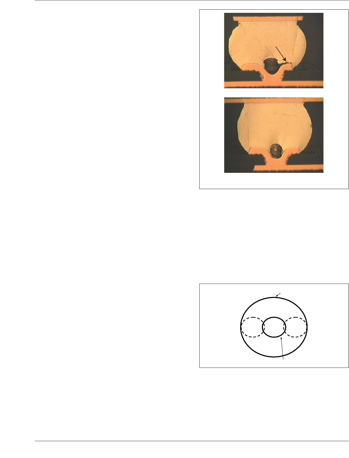
the use of designs that require lead-free assembly. Figure
A-2 shows an example as to how the cracks in the solder
joint propagates out from the void that has been created by
the absence on material in the land. This condition can be
overcome if the via is filled and over-plated so that air
entrapment does not promote this condition. Via-in-pad
designs require a further restriction of void allowance as
shown in Table A-3.
Process control criteria for the number and size of voids
discourage a general presence of voids, which indicates an
out of control process and calls for the need to use the nec-
essary tools for process and material improvement. Void
size is also important as shown in Tables A-1 to A-3 and
Figure A-3. The criteria define the characteristics for void
acceptability based on size and pitch.
For collapsible solder balls, when attached to the land pat-
tern, the ball takes an elliptical sphere form rather than a
uniform round sphere shape. Therefore, the solder joint
diameter at the ball’s center is typically greater than the
diameter at the ball-to-land interface. The criteria applied
to varying ball sizes and land sizes will result in different
void sizes.
IPC-7095c-a-2
Figure A-2 Voids in BGAs with Crack Started at Corner Lead
crack
BGA ball at 1
st
corner pin
BGA ball adjacent to 1
st
corner pin
no crack
IPC-7095c-a-3
Figure A-3 Void Diameter Related to Land Size
Solder Land Area
12% Void Area
January 2013 IPC-7095C
155
Copyright IPC-Association Connecting Electronics Industries
Provided by IHS under license with IPC
Not for Resale
No reproduction or networking permitted without license from IHS
--`,,```,,,,````-`-`,,`,,`,`,,`---
ANSI/IPC-T-50 Terms and Definitions for
Interconnecting and Packaging Electronic Circuits
Definition Submission/Approval Sheet
The purpose of this form is to keep
current with terms routinely used in
the industry and their definitions.
Individuals or companies are
invited to comment. Please
complete this form and return to:
IPC
3000 Lakeside Drive, Suite 309S
Bannockburn, IL 60015-1249
Fax: 847 615.7105
SUBMITTOR INFORMATION:
Name:
Company:
City:
State/Zip:
Telephone:
Date:
❑ This is a NEW term and definition being submitted.
❑ This is an ADDITION to an existing term and definition(s).
❑ This is a CHANGE to an existing definition.
Term Definition
If space not adequate, use reverse side or attach additional sheet(s).
Artwork: ❑ Not Applicable ❑ Required ❑ To be supplied
❑ Included: Electronic File Name:
Document(s) to which this term applies:
Committees affected by this term:
Office Use
IPC Office Committee 2-30
Date Received:
Comments Collated:
Returned for Action:
Revision Inclusion:
Date of Initial Review:
Comment Resolution:
Committee Action: ❑ Accepted ❑ Rejected
❑ Accept Modify
IEC Classification
Classification Code • Serial Number
Terms and Definition Committee Final Approval Authorization:
Committee 2-30 has approved the above term for release in the next revision.
Name:
Committee: Date:
IPC 2-30
Copyright IPC-Association Connecting Electronics Industries
Provided by IHS under license with IPC
Not for Resale
No reproduction or networking permitted without license from IHS
--`,,```,,,,````-`-`,,`,,`,`,,`---

Put IPC MEMBERSHIP to WORK for your COMPANY
Keep on top of industry developments …
and how they will affect your company
• Enjoy 24/7 privileges to FREE members-only online resources, including a
searchable archive of original articles and presentations on the latest technical
issues and industry/market trends.
• Receive FREE exclusive statistical reports available for the EMS, PCB, laminate,
process consumables, solder and assembly equipment industries.
• IPC events, including IPC APEX EXPO
TM
, technical conferences, workshops,
training and certication programs and executive management summits provide
unparalleled educational and networking opportunities.
• Stay abreast of global environmental directives, legislation and regulations, and
how these specically impact each segment of our industry’s supply chain.
Save enough money to easily pay for your
membership
• Get discounts of up to 50 percent on IPC standards, publications and training
materials.
• Save money on online subscription licenses of IPC standards through the world’s
largest standards reseller — IHS.
• Enjoy dramatic discounts on registration fees for meetings, technical
conferences, workshops and tutorials.
• B enet from preferred pricing on exhibit space at IPC trade shows and events.
“
Graphic PLC has enjoyed the privilege of being
an IPC member for more than 30 years and the
technical benefits derived to focus us as a world
player in the manufacture of PCBs have superceded
the cost of membership many times.”
Rex Rozario, OBE
Chairman
Graphic Plc.,UK
“ Being a part of the fast-changing global electronics
marketplace requires constant intelligence about
market trends, standards and solutions to the
challenges throughout the supply chain. IPC is an
invaluable partner in providing that intelligence
through conferences, white papers and technical
standards.”
Andy Hyatt
Executive Vice President
Business Development
Creation Technologies
A trusted leader for more
than 50 years, IPC is the
premier source for industry
standards, training, market
research and public policy
advocacy — supporting the
needs of the estimated $1.7
trillion global electronics
industry.
For less than $3.00 a
day, IPC members enjoy
unlimited access to the
tools, information and
forums needed to thrive in
an ever-changing electronic
interconnect industry.
“ I have a responsibility to
my customers and my
shareholders. Between the
savings on standards, training
materials, APEX and industry
data, IPC membership
provides immediate 100%
return on investment for us. It
would be irresponsible not to
be a member.”
Joseph F. O’Neil
President
Hunter Technology Corp
Copyright IPC-Association Connecting Electronics Industries
Provided by IHS under license with IPC
Not for Resale
No reproduction or networking permitted without license from IHS
--`,,```,,,,````-`-`,,`,,`,`,,`---