IPC-7095C-2013.pdf - 第22页
for the routing requirements for the organic high-density microcircuit board manufacturer . In addition, underfill is usually required to accommodate and soften the mismatch between the coef f icient of thermal expansion …
Placing signal pin assignments on the outer rows of an
array package, and using the inner balls for power and
ground will facilitate escape routing. However, the corner
balls of large array packages are more susceptible to
mechanical failure and, therefore, it may be better to use
these for redundant ground connections. The number of
rows of signal I/O that can be routed out will depend on the
desired number of conductor routing layers in the printed
board and the number of conductors that can be routed
between lands and vias.
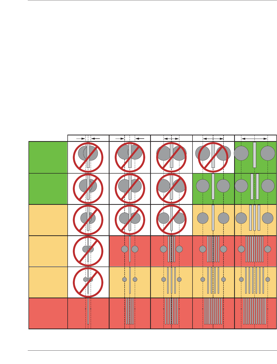
Figure 3-5 shows examples of conductor and space widths
that will fit between adjacent lands with various pitches
and land diameters. Note that as the ball pitch decreases,
the conductor width and spacing for a given number of
conductors per channel also decreases, and it becomes
more difficult and costly to produce the board.
Using 150 µm conductors and spaces is quite cost effective,
but printed board cost begins to increase significantly for
100 µm conductors and spaces. Using an organic intercon-
necting substrate to mount the bare die within a plastic
BGA requires that the mounting lands on the substrate
match the bonding lands on the die.
The bonding lands are typically positioned for wire bond-
ing, since this is the most popular technique. Thermally
conductive adhesive is one of the methods used to attach
the back of the die to the substrate. Depending on the
number of I/O and the lead pitch, multilayer substrate fab-
rication techniques may be used to translate a peripheral
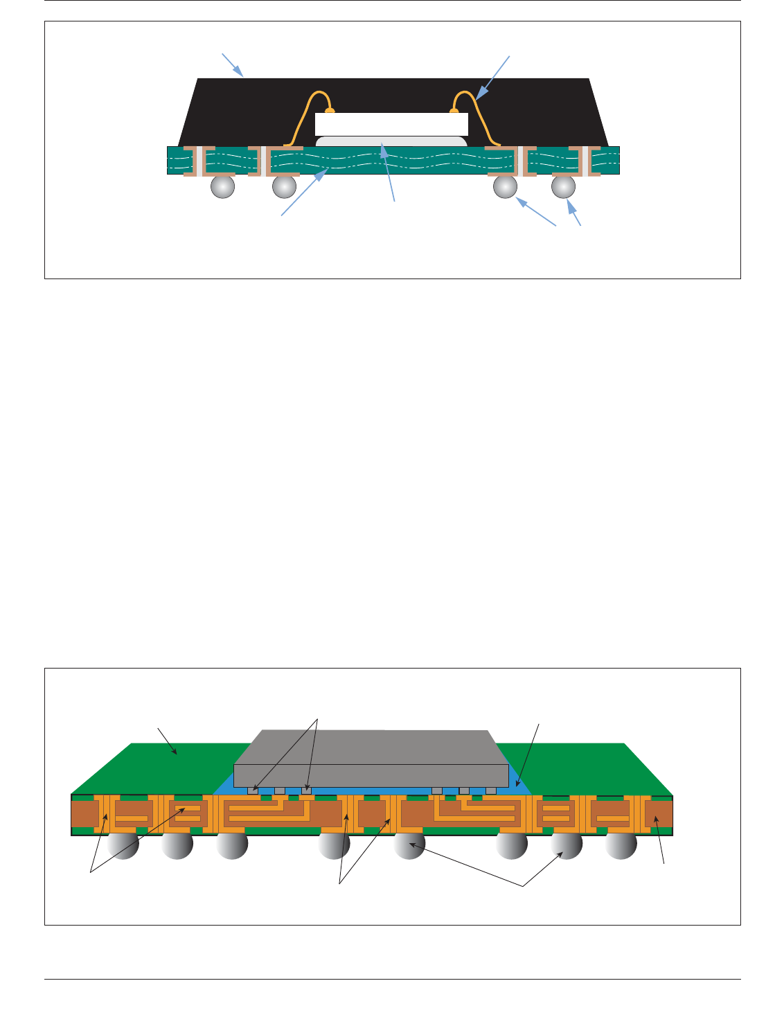
bonding land die, to an area array matrix of bumps, balls,
or columns (see Figure 3-6).
The transition of chip bonding lands that are in an array
format permits the mounting of the die in flip chip configu-
rations. In this instance, the die is mounted opposite to that
which is wire-bonded and the bumps of the die come into
direct contact with the substrate being used to convert the
die pattern to the BGA pattern. This creates new challenges
Figure 3-5 Conductor Width to Pitch Relationship
Conventional FR-4
125 µm Line
125 µm Space
700 µm Land
Conventional FR-4
125 µm Line
125 µm Space
600 µm Land
High Density FR-4
100 µm Line
100 µm Space
600 µm Land
Next Gen FR-4
60 µm Line
50 µm Space
300 µm Land
Next Gen Microvia
50 µm Line
50 µm Space
50 µm Land
Typical Microvia
75 µm Line
100 µm Space
200 µm Land
0.25 mm Pitch 0.5 mm Pitch 0.75 mm Pitch 1.0 mm Pitch 1.27 mm Pitch
January 2013 IPC-7095C
7
Copyright IPC-Association Connecting Electronics Industries
Provided by IHS under license with IPC
Not for Resale
No reproduction or networking permitted without license from IHS
--`,,```,,,,````-`-`,,`,,`,`,,`---
for the routing requirements for the organic high-density
microcircuit board manufacturer. In addition, underfill is
usually required to accommodate and soften the mismatch
between the coefficient of thermal expansion (CTE) of the
chip and the CTE of the organic multilayer board (see
Figure 3-7).
3.1.3 Assembly Equipment Impact Implementing BGA
technology may require some new assembly capability.
Depending upon the type of pick and place systems, a
change in package carrier mechanism may also be required
to transfer packages from matrix tray to the pick position.
Fiducials may also help vision systems recognize the exact
location of the land pattern for the BGA, similar to what is
used for fine-pitch peripheral leaded parts. Large BGA
parts on tape-and-reel will require 44 mm and 56 mm feed-
ers depending on the body size. Use of a forced air convec-
tion oven is preferred. Repair and inspection of BGAs are
rather difficult. Rework machines with paste deposition,
preheat, and vision capability may not be required, but are
very helpful. X-ray and optical inspection (endoscope)
capability for process development is a benefit.
3.1.4 Stencil Requirements The stencil thickness may
need to be reduced when using finer pitch BGA parts. Sten-
cil thickness and land size will determine paste volume,
which is very critical for ceramic BGAs. It is helpful to
have trapezoidal stencil apertures (slightly larger opening
on the bottom than on the top) for better paste release.
Generally, on larger BGA components with 1.25 mm and
1.00 mm pitch, the aperture is large enough that stencil
clogging, print registration and definition are less of a prob-
lem than with quad flat pack (QFP) components.
Matching solder paste stencil openings to the requirements
of fine-pitch BGAs requires an understanding of the rela-
tionship between the stencil aperture and the size of the
particles in the paste. IPC-7525 provides good descriptions
to help make the appropriate relationship decisions as the
land patterns for attachment become smaller and are closer
to one another.
Overmolded Epoxy
BT Substrate
Wire Bonds
Die Attach
Solder Balls
(Sn63Pb37)
Silicon Die
IPC-7095c-3-6
Figure 3-6 Plastic Ball Grid Array, Chip Wire Bonded
IPC-7095c-3-7
Figure 3-7 Ball Grid Array, Flip Chip Bonded
High Melt Temperature Solder
or Z-Axis Interconnection Material
Soldermask
Epoxy Underfill
Copper Circuitry
and Plated Vias
Thermal Vias
Solder Balls
IC chip
High Performance
Laminate Material
IPC-7095C January 2013
8
Copyright IPC-Association Connecting Electronics Industries
Provided by IHS under license with IPC
Not for Resale
No reproduction or networking permitted without license from IHS
--`,,```,,,,````-`-`,,`,,`,`,,`---

3.1.5 Inspection Requirements As with any surface
mount part, BGAs should not be moved after component
placement because this may smear the paste and cause sol-
der bridges. Even if some misalignment is visually
observed, many parts will self-align during reflow if their
terminations are no more than 50% off the land. If a BGA
has a gross misalignment problem, it should be removed
before reflow and reworked later. Though it may not be
practical for high volume production, using X-ray or opti-
cal inspection (endoscope) to inspect failures before
removing the part may be desirable.
3.1.6 Test Test strategies need to be developed before
using BGAs. The solder joints cannot be probed and test
points are required. It may be difficult to incorporate
enough test points to adequately test all solder joints. Some
alternative test strategies may be needed such as designing
BGA components with boundary scan capability designed
into them reducing the number of I/O fanout probe points.
In an effort to improve test capability, some BGA compo-
nents had test points designed right on the top of the pack-
age. This was not a good solution since it put pressure on
the BGA components and the joints.
3.2 Time-to-Market Readiness Before implementing
BGAs into products, it is important to address not just the
technical issues, but also the possible business implica-
tions. It is very likely that time-to-market will be adversely
impacted if both products and the technology are devel-
oped simultaneously. It is a good idea to first develop and
validate the technology before implementing it on a real
product. Otherwise, if any problem develops in the product
or technology, the deadline for product shipment will be
missed. To assure time-to-market readiness, BGA imple-
mentation methodology and process steps should be ana-
lyzed.
3.3 Methodology Several factors must be considered
when making design decisions in an attempt to balance
size, cost, and functionality. In addition to these consider-
ations, the product must also be able to perform reliably
over the expected lifespan of the product in its intended
environment. Package selection may be influenced by these
reliability factors and environmental conditions such as
temperature vibration, shock, and humidity.
3.4 Process Step Analysis There are several available
paths to utilizing BGAs effectively. The length of each path
depends on what design and assembly facilities a company
presently has, and how quickly they can be made ready for
production. The following is an example of one approach:
1. Select a list of candidate products for BGAs.
2. Develop an equipment list based on the projected vol-
ume needs. If sufficient in-house expertise does not
exist, it may be desirable to use a reputable training
center or consultant to save cost and time.
3. Organize a team representing design, production, test,
quality, and purchasing. This team is responsible for
component and equipment selections and review.
4. Develop a comprehensive BGA design guide that
stresses manufacturability. Use existing standards where
possible.
5. Design the candidate products starting with the conver-
sions of existing products using fine pitch components.
6. Determine the need for lead-free products including the
alloy used on the part as well as the surface finish
needed on the mounting substrate.
7. Conduct rigorous assembly and test reviews. Carefully
monitor component purchasing to assure that compo-
nents have the specified package, shipping method, met-
allization, solderability, and orientation in the shipping
containers.
8. Develop comprehensive workmanship standards and a
process control system that is statistically sound.
9. Design the remaining candidate products.
With the major emphasis on using parts that meet both
customer requirements and conform to new environmental
regulations, many customers are requiring reports listing all
materials used at the component level and also for com-
pleted assemblies. To help facilitate this, IPC has devel-
oped IPC-1751 and IPC-1752 on Materials Declaration,
and have encouraged software providers to make tools
available that meet the requirements of those standards.
The requirement to establish a formal declaration system
has been in place since the automotive industry was chal-
lenged by the ‘‘End-of-Life’’ European directives.
To show an example of the breadth of the variation in
material properties that may occur in products, Table 3-3
shows a list of materials that might be used as a surface
finish or a material that was added to the assembly as the
second level interconnection.
3.5 BGA Limitations and Issues Even though BGA tech-
nology has moved into the mainstream, there are still some
decisions that need to be considered. These are business
and technical issues that must be resolved. The areas of
special concern are:
• Visual inspection
• Moisture sensitivity
• Rework
• Cost
• Availability
• Voids in BGA
• Open joint (BGA or PoP BGA)
• Head-on-pillow phenomenon
• Standards and their adoption
• Reliability concerns
January 2013 IPC-7095C
9
Copyright IPC-Association Connecting Electronics Industries
Provided by IHS under license with IPC
Not for Resale
No reproduction or networking permitted without license from IHS
--`,,```,,,,````-`-`,,`,,`,`,,`---