IPC-7095C-2013.pdf - 第152页
9 DEFECT AND FAILURE ANALYSIS CASE STUDIES The following clauses identify possible assembly anoma- lies related to the assembly of BGA components. The descriptions include post process failures related to the mounting st…

Table 8-6 Accelerated Testing for End Use Environments
Worst-Case Use Environment Accelerated Testing
Use Category
Tmin
°C Tmax °C
ΔT
(1)
°C
t
D
hrs
Cycles/
Year
Typical
Years
of
Service
Approx.
Accept.
Failure
Risk %
Tmin
°C Tmax °C
ΔT
(2)
°C
t
D
min
1) Consumer 0 +60 35 12 365 1-3 1 +25 +100 75 15
2) Computers +15 +60 20 2 1460 5 0,1 +25 +100 75 15
3) Telecom -40 +85 35 12 365 7-20 0,01 0 +100 100 15
4) Commercial
Aircraft
-55 +95 20 12 365 20 0,001 0 +100 100 15
5) Industrial &
Automotive
Passenger
Compartment
-55 +95 20
&40
&60
&80
12
12
12
12
185
100
60
20
10 0,1 0 +100 100 15
& COLD
(3)
6) Military
Ground &
Ship
-55 +95 40
&60
12
12
100
265
10 0,1 0 +100 100 15
& COLD
(3)
7) Space
leo
geo
-55 +95 3
to 100
1
12
8760
365
5-30 0,001 0 +100 100 15
& COLD
(3)
8) Military
Avionics
a
b
c
-55 +95 40
60
80
&20
2
2
2
1
365
365
365
365
10 0,01 0 +100 100 15
& COLD
(3)
9) Automotive
Under Hood
-55 +125 60
&100
&140
1
1
2
1000
300
40
5 0,1 0 +100 100 15
& COLD
(3)
&
LARGE ΔT
(4)
& = in addition
1)
ΔT represents the maximum temperature swing but does not include power dissipation effects; for power dissipation calculate ΔT; power dissipation can make
pure temperature cycling accelerated testing significantly inaccurate. It should be noted that the cyclic temperature range, ΔT is not the difference between
the possible minimum, T
min
and maximum, T
max
, operational temperature extremes; ΔT is typically significantly less.
2)
All accelerated test cycles shall have temperature ramps, 20°C/minute and dwell times at temperature extremes shall be 15 minutes measured on the test
boards. This will give ~24 test cycles/day.
3)
The failure/damage mechanism for solder changes at lower temperature; for assemblies seeing significant cold environment operations, additional ‘‘COLD’’
cycling, from perhaps -40 to 0°C, with dwell times long enough for temperature equilibration and for a number of cycles equal to the ‘‘COLD’’ °C operational
cycles in actual use is recommended.
4)
The failure/damage mechanism for solder is different for large cyclic temperature swings traversing the stress-to-strain -20 to +20°C transition region; for
assemblies seeing such cycles in operation, additional appropriate ‘‘LARGE ΔT’’ testing with cycles similar in nature and number to actual use is
recommended.
January 2013 IPC-7095C
137
Copyright IPC-Association Connecting Electronics Industries
Provided by IHS under license with IPC
Not for Resale
No reproduction or networking permitted without license from IHS
--`,,```,,,,````-`-`,,`,,`,`,,`---
9 DEFECT AND FAILURE ANALYSIS CASE STUDIES
The following clauses identify possible assembly anoma-
lies related to the assembly of BGA components. The
descriptions include post process failures related to the
mounting structure characteristics and the variation in the
solder ball used as the BGA termination. In many instances
attachment metallurgy are discussed especially if the char-
acteristics contributed to the joint failure. Final joint con-
figurations are also analyzed.
9.1 Solder Mask Defined BGA Conditions There are
two ways BGA Lands are defined: solder masked defined
(SMD) where the land size is larger than solder mask and
the molten BGA ball touches the solder mask after reflow.
The other method for designing the BGA land is called
etched or nonsolder mask defined (NSMD) where the mask
opening is larger than the copper land and hence the ball
does not touch the solder mask after reflow. This condition
is shown in 9.1.1 and 9.1.2.
Solder mask-defined lands may be used on corresponding
noncritical or functional pins, since SMD lands can help
minimize pad cratering defects. However, it should be
understood that solder mask defined lands create additional
stress initiation sites and should be avoided on both the
interposer and the printed board land.
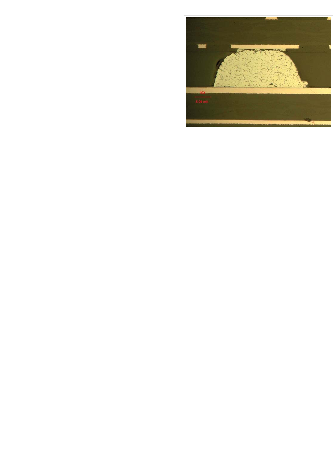
9.1.1 Solder Mask Defined and Nondefined Lands
Possible Cause
Interposer is solder mask defined; board is metal-defined. If the
two areas are very different, the stresses are not uniform and
cracks may occur at the solder mask defined side. Board land
pattern too large.
Potential Solution
Area of the two attachment conditions should be similar or
identical. In addition, solder mask defined lands create addi-
tional stress initiation sites and should be avoided on both the
interposer and the printed board land.
IPC-7095C January 2013
138
Copyright IPC-Association Connecting Electronics Industries
Provided by IHS under license with IPC
Not for Resale
No reproduction or networking permitted without license from IHS
--`,,```,,,,````-`-`,,`,,`,`,,`---
9.1.2 Solder Mask Defined Land on Product Board
The main disadvantage of solder mask defined land is that
the stress concentrations created by SMD (solder mask
defined) solder joint can be the origin of solder joint fail-
ures and reduced reliability. This condition is shown in
9.1.3. For equal solder joint height, increases in fatigue life
by factors of about 1.25 to 3 can be anticipated with the
use of nonsolder mask defined (NSMD) vs. SMD lands,
with the larger improvements for solder joints with the
more severe loading conditions.
There are three main disadvantages of SMD lands:
• Less real estate for topside breakout
• Loss of accuracy of land dimension
• Reduced reliability as it is the origin of early solder joint
failure
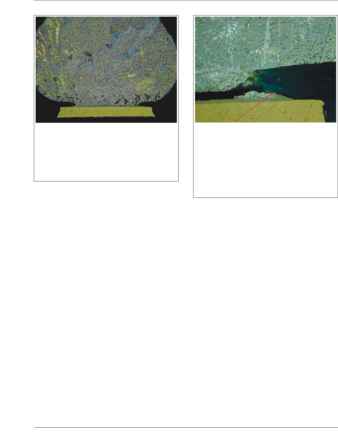
9.1.3 Solder Mask Defined BGA Failures
Possible Cause
Solder mask encroaches too far on land at board level. This
condition creates stresses in the ball that can propagate a
crack during temperature changes.
Potential Solution
Always design product boards using only metal-defined
(NSMD) lands, unless a solder mask defined land is needed to
reduce the incidence of pad cratering.
Crack starts in the solder and eventually travels down to
and through the intermetallic layer. Nickel buildup under
the solder mask is also evident.
Possible Cause
Crack starts in solder at sharp corner of solder mask. The con-
dition due to stresses in the ball caused crack propagation.
Potential Solution
Always design product boards using only metal-defined
(NSMD) lands, unless a solder mask defined land is needed to
reduce the incidence of pad cratering.
January 2013 IPC-7095C
139
Copyright IPC-Association Connecting Electronics Industries
Provided by IHS under license with IPC
Not for Resale
No reproduction or networking permitted without license from IHS
--`,,```,,,,````-`-`,,`,,`,`,,`---