IPC-7095C-2013.pdf - 第156页
9.2.8 Eggshell Void 9.3 BGA Interposer Bow and Twist Plastic BGAs have a tendency to warp during normal assembly reflow pro- cesses. The warpage can occur on the BGA substrate or on the product PCB. The result can be an o…
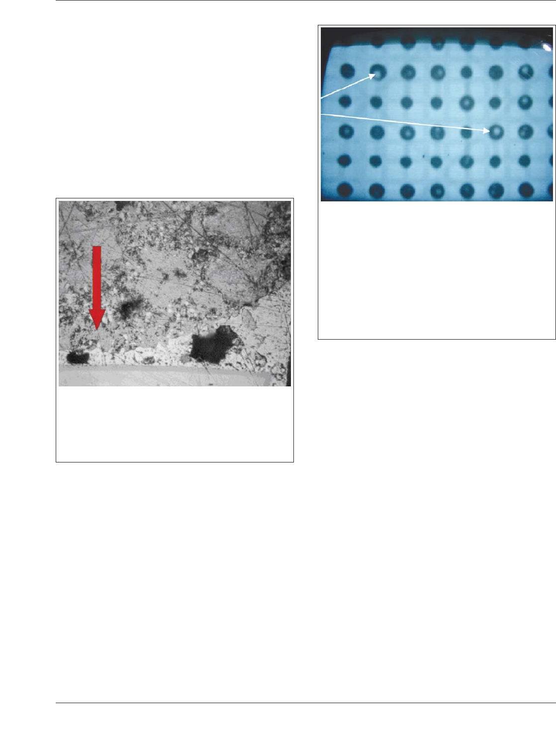
9.2.4 Critical Solder Paste Conditions The amount of
solder paste deposited for plastic BGA attachment is help-
ful, but not very critical in formation of good solder joint
since the ball itself can be the source of solder. However,
in the case of ceramic BGA (CBGA), it is very important
that enough solder paste is deposited. The recommended
volume of solder paste for 890 µm CBGA is 0.12 cubic
mm and 0.08 cubic mm minimum. If sufficient solder paste
is not deposited, as shown in 9.3.1, the reliability of solder
joint may be questionable. The reason solder must be
added to the high temperature solder ball or column is that
there is no contribution of solder volume from the package
termination to the solder joint.
9.2.5 Overly Thick Paste Deposit
9.2.6 Void Determination Through X-Ray and Cross-
Section
Transmission X-ray can detect void presence
(light areas) and the associated X-Y location. The tech-
nique can also detect uneven or missing solder balls (vari-
ous dark image diameters). An example of this condition is
shown in 9.2.7. However, cross-section X-ray is required to
determine the vertical (Z axis) location of the void in the
solder joint.
9.2.7 Voids and Uneven Solder Balls
There are many reasons for formation of voids in BGA.
However, the presence of voids does not pose any reliabil-
ity risks. Voids, as shown in 9.2.8, can survive 1000 ther-
mal cycles (no shock, 0-100°C), although more common
voids are shown in 9.2.7. Even though voids do not reduce
the fatigue life results in some tests, the presence of exces-
sive voids in solder joints is an indication of design,
process or materials issues. Product reliability should also
be verified.
Possible Cause
Thicker paste was intended for a ceramic noncollapsible ball,
not a plastic BGA ball.
Potential Solution
Reduce stencil thickness; microetch down at BGA area; reduce
stencil opening.
Possible Cause
– Excess voiding in solder ball attachment.
– Via in pad design (voids related to via in pad design are not
considered a defect as per IPC-A-610).
– Fast ramping profile.
– Forward compatibility scenarios (tin/lead BGA ball with Lead
Free Solder Paste).
Potential Solution
– Evaluate structural strength of joint through thermal stress or
microsection.
– Use reflow profile with long soak.
– Avoid situations noted under potential causes.
January 2013 IPC-7095C
141
Copyright IPC-Association Connecting Electronics Industries
Provided by IHS under license with IPC
Not for Resale
No reproduction or networking permitted without license from IHS
--`,,```,,,,````-`-`,,`,,`,`,,`---
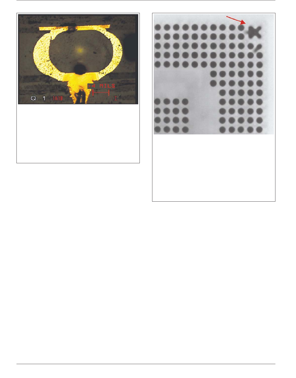
9.2.8 Eggshell Void
9.3 BGA Interposer Bow and Twist
Plastic BGAs have a
tendency to warp during normal assembly reflow pro-
cesses. The warpage can occur on the BGA substrate or on
the product PCB. The result can be an open or short con-
dition at the solder joint that deals with the stresses. The
temperature (reflow profile), BGA construction, solder
paste volume, and cooling condition all contribute to the
possible defect. Shorts in the corner balls, is an indication
of warpage in BGA where the corners of the BGA package
are bent inward (frowning BGA).
Solder shorts are caused in adjacent and/or opposite BGA
corners as the substrate bows downward (frowning) and
applies a stress to the corner balls. This same phenomena
can cause balls, away from the corner, to lift away from the
mounting substrate as the substrate changes from frowning
to smiling as shown in 9.3.1 and 9.3.2. As BGA substrates
and die are becoming thinner, package warpage is increas-
ing. In order to have a robust SMT process, checking to see
that sufficient solder paste has been added to the land is
recommended. The process should be closely monitored to
ensure that additional defects are not created such as solder
bridging, solder balling, etc.
9.3.1 BGA Interposer Warp
Opens in corner balls is an indication of warpage in BGA
where the corners of the package are lifted upward. Such
opens, as shown in 9.3.2, could be minimized by using an
extra amount of solder paste.
Adding excess solder is not a solution to the problem.
Determining the root cause and addressing the reasons for
the anomaly is more important toward establishing a robust
process. Modifying the stencil aperture to permit solder
paste deposits on the board should be used as a solution to
open corners only when certain process or component con-
ditions cannot be altered, such as when the reflow process
has already been optimized, the BGA package or the BGA
interposer cannot be redesigned, or the product board can-
not be redesigned. In addition, the anomaly must consis-
tently occur and solder and component inventory should be
considered prior to making any process changes. If the
decision is made to use excess solder paste to correct opens
in corner balls, the process should be closely monitored to
insure that additional defects are not created such as solder
bridging, solder balling, etc.
Microvia 0.65 mm @ 1000 cycles
Shows collapse of solder joint, intermittent contact fail-
ure resulted
Possible Cause
Entrapment of air or other gaseous species during reflow. The
air or other gaseous species could possibly have evolved from
the microvia in the PCB.
Potential Solution
Remove component and replace with new one.
Possible Cause
– Warpage of the BGA caused by thermal mechanical stresses
during reflow soldering.
– Check other corners for similar conditions.
– May be caused by frowning BGA interposer where the corner
becomes raised.
Potential Solution
– Increase ball size at corner or use glue-dot. In some
instances add in tape during the reflow process.
– Return package to supplier.
– Check coplanarity using shadow moiré at reflow temperature.
IPC-7095C January 2013
142
Copyright IPC-Association Connecting Electronics Industries
Provided by IHS under license with IPC
Not for Resale
No reproduction or networking permitted without license from IHS
--`,,```,,,,````-`-`,,`,,`,`,,`---
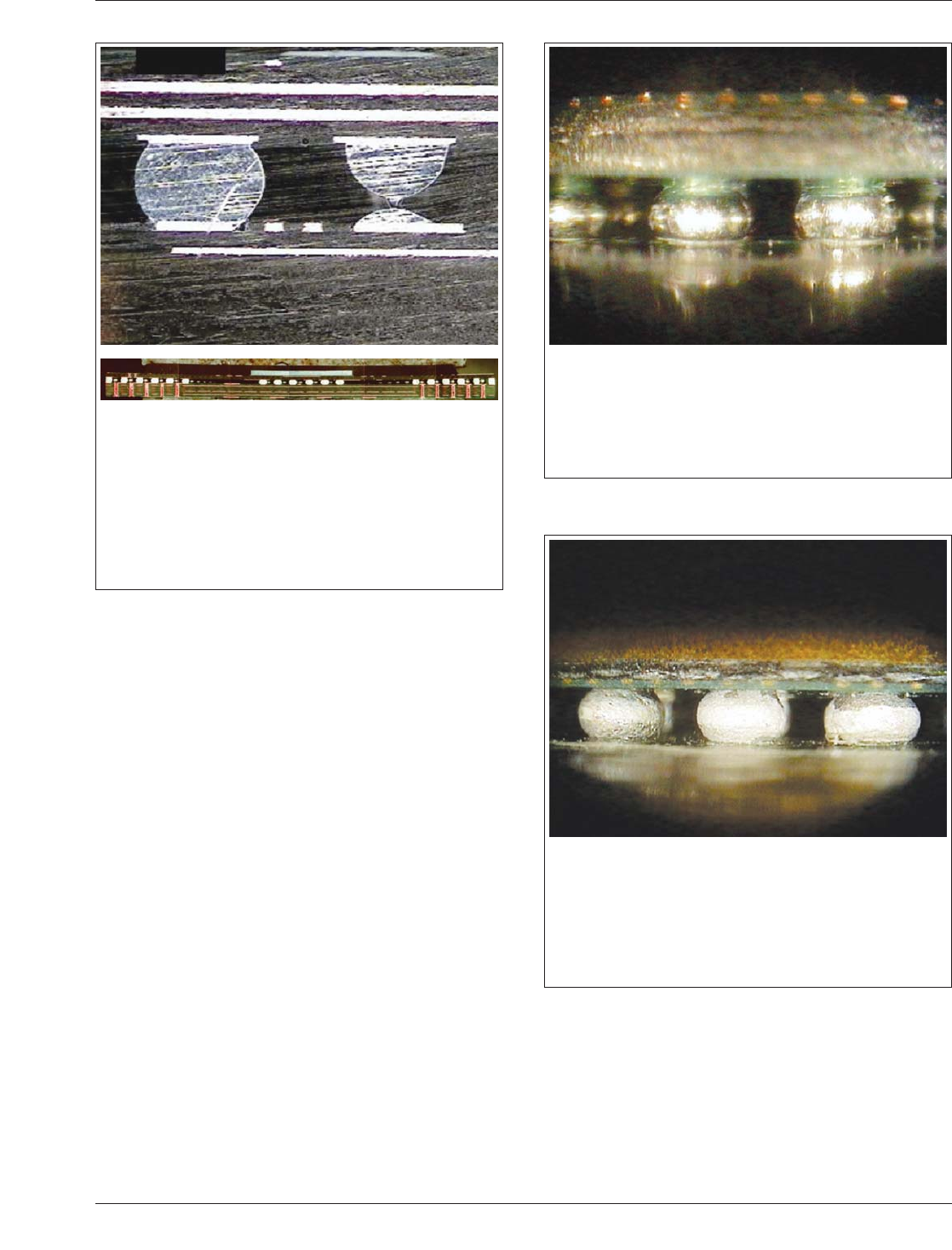
9.3.2 Solder Joint Opens Due to Interposer Warp
9.4 Solder Joint Conditions
The following sections deal
with the conditions of the solder ball in relationship to the
mounting structure and the component interposer. In each
instance, an explanation is provided as to the reason for the
occurrence of the condition.
9.4.1 Target Solder Condition
9.4.2 Solder Balls with Excessive Oxide
Possible Cause
– The failure appears to be due to insufficient paste release
from the stencil or insufficient ball size.
– Warped package (smiling BGA) with corner balls lifted up.
Potential Solution
– Check balls at incoming prior to assembly.
– Return package to supplier.
– Implement incoming inspection and/or source audit.
– Apply extra solder paste on corner lands.
Possible Cause
Solder balls exhibit a uniform shape and texture, and they are
symmetrically aligned to the attachment sites, showing ball col-
lapse on both top and bottom of BGA balls.
Potential Solution
Document process parameters and maintain a stable process.
Possible Cause
Solder ball oxides will form due to exposure to multiple reflow
solder cycles (topside or bottom side).
Potential Solution
This can be reduced significantly by correct flux selection,
reducing the number of production reflows to two and not
cleaning the PWB between reflows.
January 2013 IPC-7095C
143
Copyright IPC-Association Connecting Electronics Industries
Provided by IHS under license with IPC
Not for Resale
No reproduction or networking permitted without license from IHS
--`,,```,,,,````-`-`,,`,,`,`,,`---