IPC-7095C-2013.pdf - 第18页
components fall into this category , while only 5% of all components used have over 208 I/Os, the cross-over point between peripheral leaded component style packages and array type formats. Many peripherally leaded, lowe…
mounting substrate. With the exception of no-clean fluxes,
cleaning problems arise with fine-pitch devices that sit
almost flush (less than 250 µm) to the board. For proper
cleaning, a 0.4 mm to 0.5 mm standoff is recommended,
with the need to meet this requirement based on the size of
the BGA package, since smaller profiles allow easier pen-
etration of the cleaning solutions. Using a temporary solder
mask over the vias under a package avoids flux entrapment
problems. However, this extra process step increases pro-
duction cost.
3.1 Description of Infrastructure The use of BGAs in
the design through assembly processes has become com-
mon in the last few years. Nevertheless, incorporating these
parts into electronic assemblies requires dedicated engi-
neering resources to develop, implement and integrate the
processes into the assembly operation. Even though BGAs
can leverage existing SMT infrastructure, there are techni-
cal considerations that must be addressed in order to be
successful in implementing BGA components into existing
product configurations.
3.1.1 Land Patterns and Circuit Board Considerations
Land patterns are copper areas on the surface of the printed
board which provide the mechanical attachment for the
component and the electrical connection for its leads or
terminations. Land patterns are important to manufacturing
because the dimensions of the land affect the consistency
and reliability of the resulting solder joint, and may also
affect cleaning and testability. Land pattern design for grid
array components is even more critical because of the
increased difficulty in solder joint inspection and repair/
rework. Land pattern design issues for BGA need to be
understood. This is essential to assure proper solder joint
formation and prevent defects such as bridging, opens and
to achieve optimal reliability. Land pattern development
was difficult in the past because of the lack of standardiza-
tion in physical sizes of components, and also in the toler-
ances that were considered acceptable. There has been a lot
of effort to standardize recently, and rules for developing a
three-tiered approach to different land pattern design can be
found in IPC-7351 Generic Requirements for Surface
Mount Design and Land Pattern Standard.
BGA lands can be solder mask defined (SMD) where the
solder mask overlaps the land, or metal defined (MD)
where the solder mask stays away from the land. There are
pros and cons of each approach and the choice often
depends on the pitch of the BGA (impacting land size), or
the size of the BGA (impacting part mass). These condi-
tions help define thermal stress reliability where the MD
solder mask avoids the possibility of a stress crack in the
collapsed ball or mechanical shock reliability where the
SMD solder mask helps to secure the land to the laminate.
Both the board manufacturer and the assembler must deal
with land size issues, compatible surface finishes, solder
mask registration and electrical testing. But the assembler
has additional challenges related to the selection of appro-
priate solder alloys and paste properties, and the develop-
ment of temperature profiles and consistent processes for a
wide variety of board types and component styles.
Although the electronics industry continually reports the
development of new component packages with higher and
higher pin counts, the components with the highest usage
have pin counts in the 16 to 64 I/O range. Over 50% of all
Die Attach
Known
Good
Die
Start
Wire Bond Mold Package
Chip Attach
using Flip Chip Process
Underfill Die
Print Flux
or Paste
on BGA
Substrate Lands
Place Balls
on BGA
Substrate Lands
Perform
Electrical
Test
Inspect Pack Ship
Ball Attach
Reflow Balls on
BGA Substrate Lands
IPC-7095c-3-1
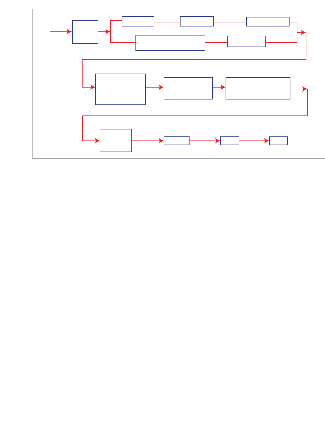
Figure 3-1 BGA Package Manufacturing Process
January 2013 IPC-7095C
3
Copyright IPC-Association Connecting Electronics Industries
Provided by IHS under license with IPC
Not for Resale
No reproduction or networking permitted without license from IHS
--`,,```,,,,````-`-`,,`,,`,`,,`---

components fall into this category, while only 5% of all
components used have over 208 I/Os, the cross-over point
between peripheral leaded component style packages and
array type formats. Many peripherally leaded, lower I/O
count devices, such as memory and logic devices, have
been converted to area array packaging formats as either
BGAs or fine pitch BGAs or some similar version of a bot-
tom only termination (see IPC-7093).
Although the percentage of high I/O components used on
an electronic assembly is small, they play a big part in
driving the industry infrastructure for both bare board and
assembly manufacturing. These high I/O components
determine the process for bare board imaging, etching, test-
ing and surface finishing. They determine the materials
used for fabrication and drive assembly process improve-
ments in a similar manner. In addition to land design, one
should also keep in mind that the inner rows of BGA pins
require additional layers for interconnection. Increasing the
number of pins (vias) drives layer count due to the reduc-
tion of routing channels. Higher layer count means higher
cost of the bare board. The electronics industry has evolved
from using through-hole assembly technology in which the
component leads went into the printed board substrate and
were either soldered to the bottom side of the board or into
a plated-through hole. Surface Mount Technology (SMT)
has advanced to a stage where the majority of electronic
components manufactured today are only available in SMT
form.
Manufacturing products with SMT in any significant vol-
ume requires automation. For low volume, a manually
operated machine or a single placement machine may be
sufficient. High volume SMT manufacturing requires spe-
cial solder paste deposition systems, multiple and various
placement machines, in-line solder reflow systems and
cleaning systems.
The heart of surface mount manufacturing is the machine
that places the components onto the printed board land
areas prior to soldering. Unlike through-hole (TH) insertion
machines, surface mount placement machines are usually
capable of placing many different component types. As
design densities have increased, new SMT package styles
have evolved. Examples are fine pitch technology (FPT),
ultra fine pitch technology (UFPT), and array surface
mount (ASM). This latter category consists of the many
families of ball or column grid arrays, chip scale packages
(CSP), fine pitch BGAs (FBGA), and flip chip (FC) appli-
cations. These parts are all capable of being placed by
machines provided that the equipment has the required
positioning accuracy.
Increased device complexity has been a primary driving
factor for SMT. In order to minimize the component
package size, component lead spacing has decreased (e.g.,
1.27 mm to 0.65 mm). Further increases in semiconductor
integration requiring more than 196 I/Os can drive pack-
ages to even closer perimeter lead spacing, such as 0.5, 0.4,
0.3, and 0.25 mm. However, the array package format has
become the favorite for high I/O count devices. Area array
component package styles have a pitch that originally was
much larger than the equivalent peripherally leaded device;
however, that lead format is now also seeing reductions in
pitch configurations.
Ball and column grid arrays were standardized in 1992
with 1.5, 1.27 and 1.0 mm pitch. Fine pitch BGA array
package standards have established pitches of 1.0, 0.8,
0.75, 0.65, and 0.5 mm. There are some implementations
of FBGAs where the pitch has been reduced to 0.4 mm,
and future components are being evaluated with 0.3 and
0.25 mm pitch configurations. Although standard configu-
rations for BGAs and their associated land patterns exist, as
described in IPC-7351, some component manufacturers
have modified the standard configurations in order to
improve the interconnection capability in the component
substrate. The tailoring of the standard geometries makes it
important to check the manufacturer’s data sheet to deter-
mine the exact characteristics of the pitch, ball size and
depopulation (removed balls).
There is a question as to how many lead pitches are
required between 1.0 mm and 0.5 mm. Some indicate that
a 60% rule is of value where the ball diameter is 60% of
the pitch. This results in a 0.5 mm ball diameter for a
0.8 mm pitch. FBGAs would use a 0.4 mm ball diameter
for a 0.65 mm pitch. On the other hand, some feel that it
would be better to standardize a 0.3 mm diameter ball for
all FBGA packages. Standardization of a single ball size
would simplify land pattern development, allow more uni-
form routing channels on the interconnecting substrate, and
help standardize socket pin contact design interconnection
of the part I/Os. All of these conditions are affected both by
ball pitch and ball diameter. Using a standardized pitch and
ball diameter combined with the ability to remove termina-
tions that are not needed would make designs more coher-
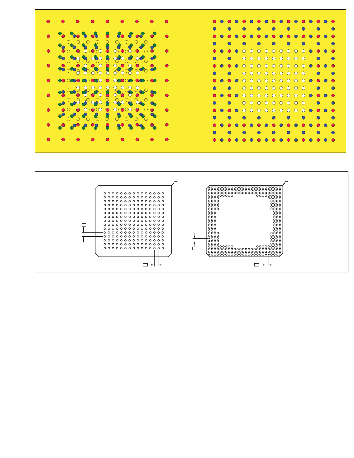
ent, as shown on the right side of Figure 3-2. The trend
illustrated on the left side of Figure 3-2 forces the creation
of many different test sockets. Interconnection of the part
I/Os is affected both by ball pitch and ball diameter. The
standard ball diameter as specified by the JEDEC JC11
Committee alleviates pressure on the substrate design.
Array packages permit a variety of ball configurations i.e.,
staggered positions or partially populated parts, to provide
the room required for adequate conductor routing. With a
common base array pitch, significant advantages can be
gained in terms of providing a coherent standard for all of
the elements of the electronic manufacturing infrastructure
for components, sockets, substrates and test systems (see
Figure 3-3). The component selection process for an elec-
tronic assembly should minimize the variation in package
types and pin pitches. Problems with the assembly of large
I/O count and fine-pitch peripheral packages has caused
IPC-7095C January 2013
4
Copyright IPC-Association Connecting Electronics Industries
Provided by IHS under license with IPC
Not for Resale
No reproduction or networking permitted without license from IHS
--`,,```,,,,````-`-`,,`,,`,`,,`---
rethinking of the relationship between packaging style and
assembly complexity, and the printed board interconnection
and surface characteristics.
The concern in using these very complex parts relates to
board design and assembly issues. Assembly is concerned
about attaching all the leads to the mounting structure with-
out bridging (shorts) or missing solder joints (opens).
Design is concerned with properly interconnecting all the
leads and having sufficient room for routing conductors.
3.1.2 Technology Comparison The principles used to
mount a single chip into an organic carrier package can
also be used to connect several chips together. This tech-
nique is referred to as a MultiChip Module-Laminate
(MCM-L) or a MultiChip Package (MCP) or the new name
assigned to complex module assemblies known as Multi
Device Subassembly (MDS). In all the variations that are
being developed, the one governing condition is the use of
the area array format. Thus, ball size and pitch will con-
tinue to be the process governing factor for individual
components or those that encompass more than one semi-
conductor die. Table 3-1 shows some examples of an
attempt to establish a definition for multichip modules
housing more than one die. Figure 3-4 is an example of one
such product using the area array concepts for interconnec-
tion.
Possible other descriptive attributes include substrate
technology (e.g., -C for ceramic, -L for laminate, -D for
deposited, -W for wafer, -S for silicon) & interconnection
technology (e.g., -WB for wire bond, -FC for flip chip,
-MX for mixed).
Microprocessors typically have between 40-60% of their
I/O dedicated to power and ground. As an example, a pack-
age might have a total of 1300-1400 I/O where the signal
count is between 600 and 700 I/O. Application Specific ICs
(ASICs) may differ in that I/O apportionment.
Figure 3-2 Area Array I/O Position Comparisons
151413121110987654321
26 24 22 20 18 16 14 12 10 8 6 4 2
25 23 21 19 17 15 13 11 9 7 5 3 1
A
B
C
D
E
F
G
H
J
K
L
M
N
P
R
T
U
V
W
Y
AA
AB
AC
AD
AE
AF
P
P
P
P
PIN #1
CORNER
PIN #1
CORNER
A
B
C
D
E
F
G
H
J
K
L
M
N
O
P
IPC-7095c-3-3
Figure 3-3 Area Array I/O Position Patterns
January 2013 IPC-7095C
5
Copyright IPC-Association Connecting Electronics Industries
Provided by IHS under license with IPC
Not for Resale
No reproduction or networking permitted without license from IHS
--`,,```,,,,````-`-`,,`,,`,`,,`---