IPC-7095C-2013.pdf - 第52页
of faithful service among the traditional resin systems. However , to support the move to meet legislated lead free requirements by the EU, many new resins are being devel- oped to meet the higher temperature assembly re…

bake-out ovens will be required. Bake-out may take
between four hours and 48 hours at 125°C or five days to
68 days at 40°C depending on package thickness and size.
In order to remove moisture from BGA components, a rec-
ommended bake cycle should be established. It should be
noted that the higher reflow temperatures required for lead-
free solders may require a more rigorous moisture removal
bake cycle.
4.8.6 Shipping Medium (Tape and Reel, Trays, Tubes)
As with all SMT components, BGA parts should be pack-
aged in Electrostatic Discharge (ESD) packaging which
meets the requirements of the appropriate standards or
specifications. BGA components should be available in
JEDEC approved matrix trays able to withstand multiple
bake cycles, as many BGAs are moisture sensitive. See
4.8.5 for required bake temperatures and times for the dif-
ferent classes of moisture sensitive components.
It may be preferable to procure high volume parts, e.g.,
SRAM or DRAM devices, in tape-and-reel for faster
assembly cycle times. Component size and moisture sensi-
tivity may dictate that tape and reel is not applicable for
some BGAs. Tape widths up to 56 mm are available, and a
tape ‘‘leader’’ of at least 200 mm should be provided. Cau-
tion must be used when baking parts in tape-and-reel, as
this type of packaging is usually restricted to lower bake
temperatures than matrix trays.
4.8.7 Solder Ball Alloy Component manufacturers
should establish a method to clearly identify the metallurgy
of the solder alloy used for the BGA balls, accompanied by
a part number change. J-STD-609 provides a convenient
method to identify the BGA ball alloy. Users may want to
verify the BGA alloy using screening methods such as
X-Ray Flourescence (XRF).
5 PRINTED BOARDS AND OTHER MOUNTING
STRUCTURES
Printed Boards (PBs) and other similar types of intercon-
nection platforms serve as mounting structures for BGAs
and other components. There is a wide variety of mounting
structures available to fulfill various interconnection sub-
strate requirements. These structures employ a wide range
of materials, both organic and inorganic and have a wide
range of physical properties. Materials are normally chosen
based on cost/performance needs of the finished product.
5.1 Types of Mounting Structures Following is an
examination of some of the more commonly used mount-
ing structure substrates.
5.1.1 Organic Resin Systems Organic substrates are
those that are most commonly used in the construction of
electronic interconnection structures. There is a well-
established worldwide manufacturing base for the organic
type of product. As a result of the large manufacturing
base, the organic materials used to create the structures
have the lowest cost among the competing technologies.
Organic materials have intrinsic beneficial electrical prop-
erties. Most notable is a relatively low dielectric constant
which can be made lower by the choice of resin and rein-
forcement. Rigid organic substrates are commonly rein-
forced with woven glass cloth. Flexible substrates are typi-
cally not reinforced.
5.1.2 Inorganic Structures Inorganic substrates are an
alternative to the organic substrates. They are commonly
refractory materials comprised of sintered metal oxides.
While they are typically brittle, they have some significant
benefits not easily obtained with organic substrates.
Chief among the advantages are excellent thermal proper-
ties. Like organic structures there are a number of possible
choices available: ceramic, silicon, and enameled metals.
The dielectric properties of these materials tend to be
higher than organic based materials and, because they are
brittle, they are generally more prone to breakage. Because
of the more limited vendor base for inorganic substrates,
these structures are normally more expensive.
5.1.3 Layering (Multilayer, Sequential or Build-Up)
While single and two metal layer circuits are still common,
multilayer interconnection structures are commonly
required to support the interconnection of BGAs in today’s
high performance electronics. There are several approaches
to creating multilayer circuit product. The traditional mul-
tilayer is created by printing and etching thin layers of
copper clad substrates and laminating them into a mono-
lithic structure which can be drilled and plated so as to
make connection between the layers where required.
More recently, however, alternative structures have been
developed to address the higher density and routing diffi-
culties associated with BGAs. These newer structures
employ a variety of different approaches to create suitable
multilayer structures. The new structures are variously
referred to as build-up multilayers, sequential multilayers
and co-laminated multilayers. A key feature of these struc-
tures is their use of very small vias. The term microvias has
been applied to describe these miniscule interconnections.
A typical microvia is less than 150 µm in diameter and has
a capture land (where the via starts) and a smaller target
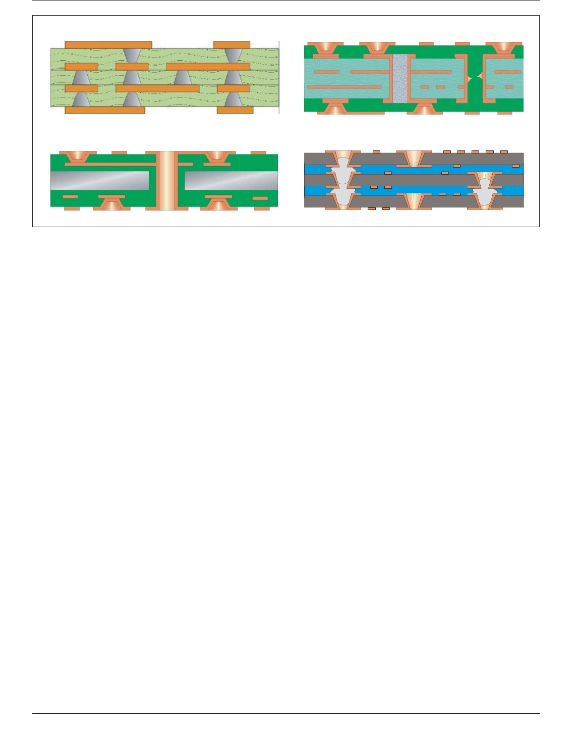
land (where the via ends). The following examples in Fig-
ure 5-1 show different high density interconnect (HDI)
printed boards (see IPC-2226).
5.2 Properties of Mounting Structures
5.2.1 Resin Systems
There are a number of different
resin systems suitable for use in organic laminate construc-
tion. There is a long and well understood history and years
January 2013 IPC-7095C
37
Copyright IPC-Association Connecting Electronics Industries
Provided by IHS under license with IPC
Not for Resale
No reproduction or networking permitted without license from IHS
--`,,```,,,,````-`-`,,`,,`,`,,`---
of faithful service among the traditional resin systems.
However, to support the move to meet legislated lead free
requirements by the EU, many new resins are being devel-
oped to meet the higher temperature assembly reflow
requirements. Test methods have been developed, i.e., Td
(Temperature of decomposition) and T260, T288, T300
(Time to Delaminate), to quantify material properties for
conformance to the new EU requirements. Some of the
new resin systems are classified to new material slash
sheets such as IPC-4101 /99, /101, /121, /124, /126 and
/129.
5.2.1.1 Epoxy Epoxy is among the organic resins with
the longest history and it is one of the most commonly used
resin systems for PCBs. It offers a good blend of physical,
electrical and processing properties at reasonable cost. The
general properties are provided in Table 5-1. Higher tem-
perature capability epoxy resin systems have been devel-
oped for lead-free applications and are available at a cost
premium.
5.2.1.2 Polyimide Polyimide offers the highest operating
temperature among resin systems in use today. It has been
a favorite for military applications where the potential for
board rework and repair in the field with uncontrolled sol-
dering tools is anticipated. Because of its high glass transi-
tion temperature, polyimide provides a safety margin and
potential to reduce damage to the board when uncontrolled
soldering irons are used to remove or replace a component.
The general properties are provided in Table 5-1.
5.2.1.3 Bismaleimide Triazine Bismaleimide triazine or
BT resin is the most popular choice for the construction of
BGA packages because of its combined advantages of high
temperature capability at reasonable cost. The general
properties are provided in Table 5-1.
5.2.2 Reinforcements Reinforcements provide the
dimensional stability and the bulk of the mechanical prop-
erties of the organic substrate laminate. Following are some
of the more commonly used reinforcements.
5.2.2.1 Glass Cloth Glass cloths are the most commonly
used reinforcement for PCB substrates. They are widely
available and are processed with relative ease. The cloths
are available in a number of different thicknesses and
weaves. The chemical make-up of the glass can vary and
can affect the electrical properties. Presently, E type glass
is the most commonly used glass cloth for PCB substrates.
5.2.2.2 Glass Felt Glass felt or nonwoven glass mat has
been commonly used as a reinforcement material for fluo-
roplastic resins and is commonly used in low loss, RF or
microwave applications. It has seen some application in
formable laminates as well.
5.2.2.3 Aramid Cloth Aramid cloth has been used to
reinforce certain laminates. It is unusual in that it has a
negative CTE in the X and Y direction which helps to off-
set the in-plane CTE of the resin. Because of the counter-
acting expansion and contraction, laminate materials of this
combination can match approximately the CTE of ceramic.
However, a drawback of the material is that the aramid has
Z-axis CTE much higher than glass and, in thermal excur-
sions, can fracture nearby resin, leaving micro-cracks along
the surface of the fibers.
IPC-7095c-5-01a,b,c,d
Figure 5-1 Examples of Different Build-Up Constructions
A. Piercing post co-laminated structure - Type IV HDI Construction
B. Sequentially built-up multilayer - Type II HDI Construction
C. Passive substrate with external microvia layers interposer - Type IV HDI Construction
D. Filled via sequentially co-laminated substrate - Coreless Type V HDI Construction
A
C
B
D
IPC-7095C January 2013
38
Copyright IPC-Association Connecting Electronics Industries
Provided by IHS under license with IPC
Not for Resale
No reproduction or networking permitted without license from IHS
--`,,```,,,,````-`-`,,`,,`,`,,`---

5.2.2.4 Aramid Paper The supply of nonwoven aramid
paper has diminished due to a lack of manufacturing
sources. Aramid papers have been effectively used in a
number of multilayer applications. They have most of the
benefits of the aramid cloth with more process latitude.
They are often used for thin core layers at or near the sur-
faces of the printed boards to better control CTE. Because
the aramid is organic, it has the added advantage of being
more easily processed by laser ablation and can also be
processed using plasma etching for making holes. The
organic nature of the material also helps to keep the dielec-
tric constant low.
5.2.3 Laminate Material Properties There are a number
of different material properties that are important in the
selection of a laminate for BGA substrate manufacture.
5.2.3.1 Thermal Expansion Thermal expansion is usu-
ally characterized in terms of changes to the x-y plane,
which is controlled primarily by the reinforcement of the
material. The x-y expansion will have the greatest effect on
surface mounted components and their reliability. Thermal
expansion also occurs in the z-axis at a rate significantly
larger than in the x-y plane, particularly at temperatures
above the T
g
. The z-axis expansion will have its greatest
effect on plated-through hole and via reliability.
Table 5-1 shows the conditions for various reinforced resin
types. All thermal expansion is measured in parts/million/
change in temperature (°C).
5.2.3.2 Glass Transition Temperature Glass transition
temperature is that property of the material where the rein-
forcement and the resin systems transition from a linear
coefficient of thermal expansion and expand at a much
higher rate. The glass transition temperature (T
g
) indicates
a temperature range within which resins change molecular
structure from a glassy to an amorphous state; these differ-
ent molecular structures result in very different physical
properties. This occurs when the resin system exceeds its
cured polymer state. It is usually an expansion in the Z-axis
of the material and the temperature stated expands at a
faster rate, although still linear (mm/mm of thickness).
Table 5-1 shows some of the characteristics of the condi-
tions for glass transition temperature of various material
types. Figure 5-2 illustrates the concept graphically and
shows how different resins might perform.
Table 5-1 Environmental Properties of Common Dielectric Materials
Environmental Property
Material
FR-4
(Epoxy
E-glass)
Multi-
Functional
Epoxy
High
Performance
Epoxy
Bismaleimide
Triazine/
Epoxy Polyimide
Cyanate
Ester
Coefficient of Thermal Expansion,
xy-plane, CTE(xy) (ppm/°C)
16-19 14-18 14-18 ~15 8-18 ~15
Coefficient of Thermal Expansion,
z-axis below T
g
1
, CTE(z,<T
g
) (ppm/°C)
50 - 85 44 - 80 ~44 ~70 35 - 70 ~81
Coefficient of Thermal Expansion
z-axis above T
g
1, CTE(z,>T
g
) (ppm/°C)
240 - 390 240 - 390 240 - 390 220 - 370 200 - 350 210 - 360
Thermal Expansion z-axis,
TE(50-260°C) (%)
3.0 - 4.5 2.5 - 4.0 2.0 - 3.5 2.0 - 3.5 1.8 - 3.0 2.0 - 3.3
Glass Transition Temperature
2
,
T
g
(°C)
110 - 140 130 - 160 165 - 190 175 - 200 220 - 280 180 - 260
Decomposition Temperature
3
,
Td (5%) (°C)
310 - 330 320 - 350 330 - 400 ~334 ~376 ~376
Soldering Temperature Impact Index
4
,
STII
170 - 205 200 - 220 215 - 260 TBD TBD TBD
Flexural Modulus (GPa)
Fill
5
Warp
6
18.6
12.0
18.6
20.7
19.3
22.0
20.7
24.1
26.9
28.9
20.7
22.0
Tensile Strength (MPa)
Fill
5
Warp
6
413
482
413
448
413
524
393
427
482
551
345
413
Water Absorption (wt%) 0.5 0.1 0.3 1.3 1.3 0.8
1. CTE (z,<T
g
) is also known as Alpha 1, and CTE(z, >T
g
) as Alpha 2. Contact supplier for specific values of the other materials.
2. The glass transition temperature can be measured by three different methods (TMA, DSC, DMA). Of these the values obtained by TMA are the most
pertinent for the purpose of assessing reliability issues. A very rough relationship between the results of these three methods is T
g
(TMA) ≈T
g
(DSC) -10°C
≈T
g
(DMA) -20°C. Contact supplier for specific values of other materials.
3. The decomposition temperature can be measured to two different values of weight loss, Td (2%) and Td (5%). Td (5%) is more commonly used, but Td (2%)
is becoming popular because of its greater usefulness. Contact supplier for specific values of other materials.
4. Soldering Temperature Impact Index, STII, which is defined as STII = T
g
/2 + Td/2 — (TE%(50 to 260°C) x 10).
5. Fill - yarns that are woven in a crosswise direction of the fabric.
6. Warp (cloth) - yarns that are woven in a lengthwise direction of the fabric.
January 2013 IPC-7095C
39
Copyright IPC-Association Connecting Electronics Industries
Provided by IHS under license with IPC
Not for Resale
No reproduction or networking permitted without license from IHS
--`,,```,,,,````-`-`,,`,,`,`,,`---