IPC-7095C-2013.pdf - 第141页
• Stif fening Mechanism • Solder V olume • Solder Mechanical Properties • Solder Creep Properties • Quality of solder Joint Interfaces As a remedy , some designers especially in the cell phone industry had adopted larger…
The dynamic warpage of the PCB and/or FCBGA stack
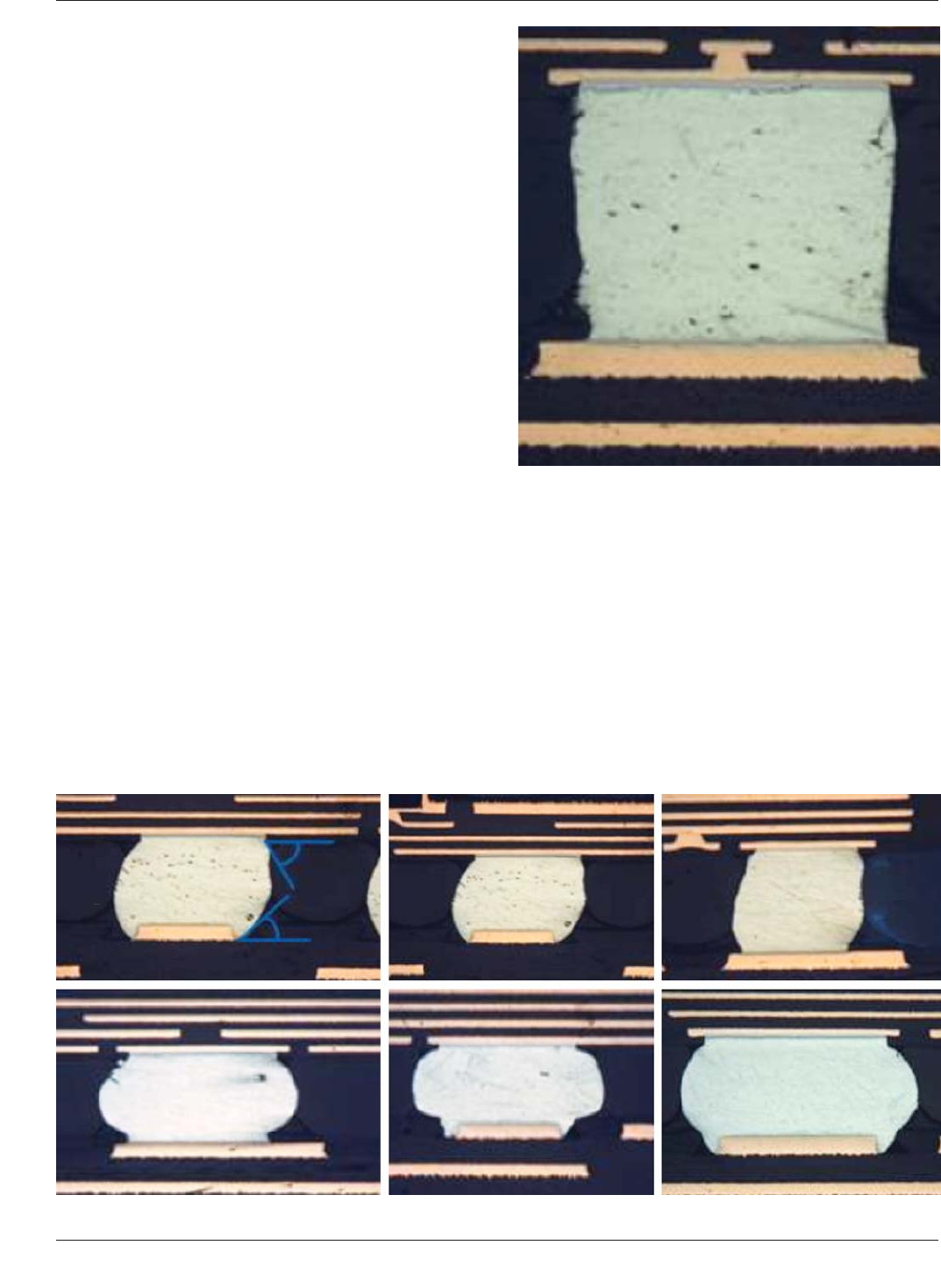
also leads to varying shapes of solder joints that are accept-
able from a quality standpoint. Figure 8-14 illustrates
examples of acceptable solder joints. Most BGA solder
joints are convex solder joints, since the smallest angle (in
blue in the top left photo of Figure 8-14) of the solder joint
surface tangent with respect to either pad surface is ≤90° at
all points along the solder joint surface.
PCB and/or BGA stack dynamic warpage can lead to some
solder joints being stretched into a columnar shape. Figure
8-15 shows an acceptable columnar solder joint. For
columnar solder joints, the solder joint surface is normal to
either side of the PCB land.
8.4.7 Failure Signature-6: Mechanical Failure Mechani-
cal stress caused by board flexing from in-circuit testing is
not uncommon in PCB assembly. As the size of the BGA
becomes larger, the stress experienced by corner joints
becomes more significant. Even probing beneath and sur-
rounding the BGA is required. Mechanical stress caused by
probe pins and vacuum force is sometimes ignored. It is
important to note that excessive monotonic stress induced
by mechanical stresses will lead to solder joint failures.
Since the weakest interface is the one that breaks, this fail-
ure signature could be different. The crack could be within
the BGA ball or at the PCB or package interface or within
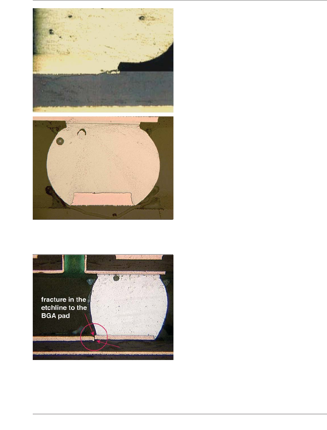
the PCB as a lifted land (pad ‘‘cratering’’). Figure 8-16
shows two examples of a lifted corner land caused by
excessive mechanical stress. This defect is also termed as
pad cratering.
Pad cratering can result in a failure of the joint due to elec-
trical opens. The initial crack weakens the joint mechani-
cally. As it progresses, the crack may intercept electrical
traces causing an open. This is shown in Figure 8-17. Fail-
ure by this signature is enhanced by the higher tempera-
tures of lead-free reflow temperatures, harder laminates,
and increasing land or trace densities.
The robustness of the BGA joints against mechanical stress
is a function of several factors:
• Location of the BGA
• Thickness of the PCB
• Stack Up
• Land Size
Figure 8-14 Examples of Acceptable Convex Solder Joints with Solder Joint Surface Tangents Shown in the Top Left Photo
Figure 8-15 Example of an Acceptable Columnar Solder
Joint
IPC-7095C January 2013
126
Copyright IPC-Association Connecting Electronics Industries
Provided by IHS under license with IPC
Not for Resale
No reproduction or networking permitted without license from IHS
--`,,```,,,,````-`-`,,`,,`,`,,`---
• Stiffening Mechanism
• Solder Volume
• Solder Mechanical Properties
• Solder Creep Properties
• Quality of solder Joint Interfaces
As a remedy, some designers especially in the cell phone
industry had adopted larger corner lands, elongated lands,
and underfill to enhance robustness. From the assembly
perspective, enforcing proper fixturing and handling are
keys to avoid solder joint damage.
8.4.8 Failure Signature-7: Insufficient Reflow This fail-
ure signature occurs when the BGA ball does not receive
sufficient heat for the solder to reach a temperature above
liquidus temperature of the solder. Insufficiently reflowed
solder joints, when they occur, are typically found under-
neath the center portion of the BGAs, because those areas
heat the slowest during soldering process, and would be the
most prone to not reaching adequate soldering tempera-
tures.
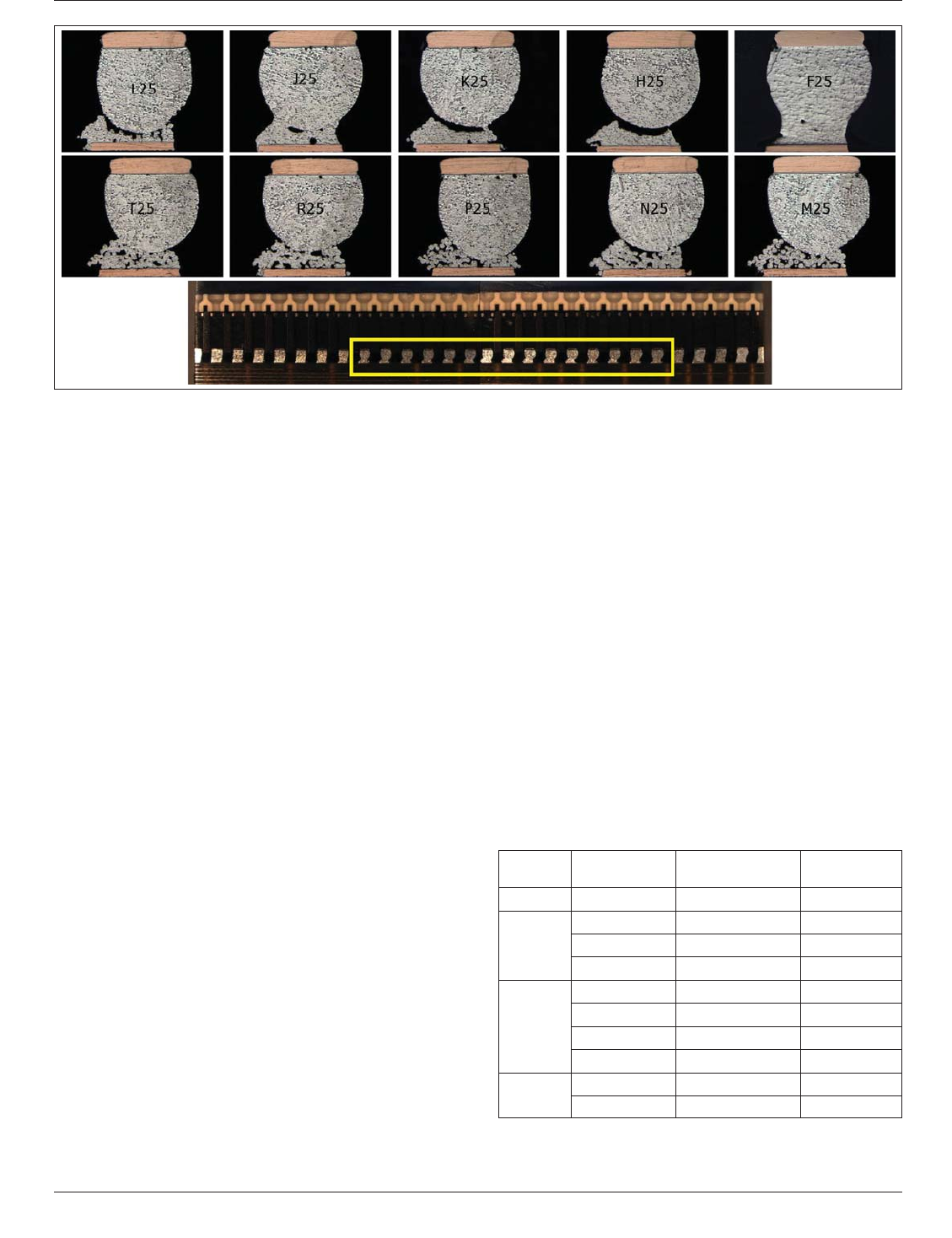
Sometimes, insufficient reflowed solder joints occur due to
the existence of a feature on a component, such as a cam
on a socket, depriving the heat from that area during the
reflow process. Figure 8-18 below illustrates an example of
insufficiently melted solder joints due to this reason.
8.5 Critical Factors to Impact Reliability
8.5.1 Package Technology
Area array components
come in a variety of styles and materials. The majority of
the commercial array devices utilize plastic encapsulation
and a reinforced rigid organic substrate interposer material
for packaging. For package-to-board interconnect, a metal-
lized land or alloy sphere (ball) is employed. Land grid
array (LGA) packaged ICs are often specified when pack-
age height is an issue, while the ball grid array (BGA) uses
small alloy spheres for the interconnect system. The con-
tact alloys furnished on the majority of the plastic based
BGA is a Sn/Pb (eutectic) or a Sn/Ag/Cu (lead-free) com-
position. Area array packages using a ceramic based sub-
strate interposer may be supplied with high-lead solder ball
or solder column, e.g., Pb90/Sn10. A growing number of
area array package variations adapt nonreinforced film
dielectric for the substrate and a diverse combination of
encapsulation materials. Miniature fine-pitch (FBGA) and
die-size package (DSP) are also widely used (especially in
portable or hand-held electronic products) and many higher
power applications incorporate an in-package heat spreader
or heat-spreading layer (see Section 4).
Long-term reliability of the solder attachment of the area
array package, when soldered to a conventional printed
board, is of primary concern. The difference in the
Figure 8-16 Two Examples of Pad Cratering (Located at
Corner of BGA)
Figure 8-17 Pad Crater Under 1.0 mm Pitch Lead-Free Sol-
der Ball. Crack in Metal Trace Connected to the Land is
Clear; However, the Pad Crater is Difficult to See in Bright
Field Microscopy.
January 2013 IPC-7095C
127
Copyright IPC-Association Connecting Electronics Industries
Provided by IHS under license with IPC
Not for Resale
No reproduction or networking permitted without license from IHS
--`,,```,,,,````-`-`,,`,,`,`,,`---
coefficient of thermal expansion (CTE) for materials can
generate undue stress to the solder interface. The solder
attachment integrity for area array packages will vary,
depending on the loading conditions to which the solder
joints are subjected and the reliability requirements for the
product. CTE mismatch is further aggravated when large
silicon die are attached to an organic substrate with a non-
compliant epoxy compound. Silicon CTE is near 3 ppm/°C
while the organic substrate is closer to 16 ppm/°C. Package
warp during assembly processing and even the power dis-
sipation within the package can subject the solder joints to
significant tensile stresses. Excessive stress and strain at
the solder interface will cause solder joint failure and even
separation of the metallized lands.
When the die is attached to the package substrate with rigid
epoxy, the substrate material directly beneath the die may
be restricted to a CTE nearer that of the die. When solder
balls are retained in the same zone and exposed to a wide
variable of operating temperature, the solder interface will
be subjected to excessive strain. For ‘‘cavity-up’’ compo-
nents (die attached facing away from the package sub-
strate), only a thin dielectric layer separates the solder
joints from the die. The larger the die is, the more acute the
concerns for solder attachment reliability. Furthermore,
when the BGA solder joints fracture, they are typically near
the ball-to-package interface. This is a consequence of the
local expansion mismatch between the solder and the die-
constrained BGA substrate.
The current trend for larger BGA package outlines is to
move the contacts toward the package perimeter, with the
possible exception of some thermal solder balls and vias
retained at the central area of the package. Several manu-
facturers that cannot move the ball contact outside the die
attach area have adapted a more compliant die attach mate-
rial. The compliant die-to-package interface is slightly
thicker and exhibits a dramatic reduction in stress at the
solder-to-board interface, furnishing a substantial increase
in fatigue life.
8.5.2 Stand-Off Height Stand-off height significantly
affects reliability of solder joints. The higher the stand-off,
the better is the reliability of solder joints. BGAs attached
with Sn63Pb37 solder balls result in solder joint heights
that are less controlled and lower (height400 to 640 µm),
while the Sn10Pb90 solder balls (diameters of 760-890 µm)
result in uniform solder joint heights of the same dimen-
sion since the Sn10Pb90 solder has a Liquidus temperature
significantly above the near-eutectic tin/lead solders and
does not melt during a typical reflow process. Table 8-2
provides information on typical stand-off heights for tin/
lead ball and solder paste metallurgy packages.
Weight of the package also affects reliability of solder joint
since it impacts solder joint or stand-off height. The key
Figure 8-18 Cross-Section Photographs Illustrating Insufficient Melting of Solder Joints During Reflow Soldering. These
Solder Joints are Located Below the Cam of a Socket.
Table 8-2 Typical Stand-Off
Heights for Tin/Lead Balls (in mm)
Ball
Pitches
Stand-off
Heights
Ball Diameter
Prior to Reflow
PCB
Land Size
1.27 0.40-0.60 0.75 0.65
1.00
0.45-0.55 0.60 0.45
0.35-0.45 0.50 0.40
0.30-0.40 0.45 0.35
0.80
0.35-0.45 0.50 0.40
0.30-0.40 0.45 0.35
0.28-0.35 0.40 0.35
0.18-0.25 0.30 0.25
0.50
0.18-0.26 0.25 0.25
0.08-0.15 0.17 0.25
IPC-7095C January 2013
128
Copyright IPC-Association Connecting Electronics Industries
Provided by IHS under license with IPC
Not for Resale
No reproduction or networking permitted without license from IHS
--`,,```,,,,````-`-`,,`,,`,`,,`---