IPC-7095C-2013.pdf - 第48页
be separated from a noisy ground where all the switching activity takes place. Some applications require several power supplies with dif ferent voltages for each part of the chip. These planes should be distributed evenl…

polyimide films are very high temperature limits (~250°C)
and relatively low dielectric constant (~3.5 versus ~4.5 for
FR-4 and ~10.0 for ceramic). In addition, it is very thin and
is much easier to produce the fine line circuit features more
commonly required for high-density area array packages.
On the negative side, the main concern with nonreinforced
or flexible materials has been their dimensional stability.
The reinforcement provides the physical characteristics that
enhance CTE properties in the X-Y axis. The X and Y axes
are the particular segments of the interconnecting product
that affect the stress on the solder joints of the package
when mounted onto the interconnecting product. In addi-
tion, polyimide film is generally more expensive than some
of the other reinforced organic base materials and it is rela-
tively hydroscopic. On the other hand, because polyimide
films are more flexible, the material will absorb rather than
transfer physical stress.
4.6.2 Properties of Substrate Materials While there are
numerous properties that are specified and measured rela-
tive to substrate materials, only a few properties are con-
sidered key to the performance of the final BGA product.
4.6.2.1 Coefficient of Thermal Expansion (CTE) The
coefficient of thermal expansion is a very important physi-
cal attribute of a BGA substrate. The CTE defines the rate
of expansion of the material with increase in temperature.
The importance is magnified when there are large differ-
ences in CTE between the BGA package and the circuit
board structure to which it is mounted. When the CTE dif-
ference is large, excessive stress and strain can be placed
on the solder ball connections resulting in accelerated sol-
der joint degradation.
4.6.2.2 Glass Transition Temperature (T
g
) The glass
transition temperature is the temperature at which the mate-
rial goes through a transformation from a rigid glass-like
state to a rubbery soft state. It is also the point at which the
material begins to lose strength and expands at a much
higher rate (i.e., the CTE increases).
4.6.2.3 Flexural Modulus Flexural modulus is important
as a measure of the stiffness or rigidity of the substrate. The
impact on the BGA is most commonly manifested in the
degree of warpage. This, in turn, can significantly impact
board assembly yield if warpage is excessive.
4.6.2.4 Dielectric Properties There are several metrics
that are included under the general heading of dielectric
properties. Dielectric constant, dissipation factor, dielectric
withstanding voltage and surface insulation resistance are
examples of such properties. These properties are impor-
tant; moreover, as computers, portable communication
products, and modules obtain higher processing capability,
signal speed and integrity become paramount. The need for
greater performance capability will be apparent as systems
designed to be run above 200-300 MHz continue to use
FR-4. As processing speeds continue to increase, it is nec-
essary to lower the dielectric constant and also lower the
dissipation factor of the material. The more advanced sub-
strate material systems can provide robust solutions. For
example, cyanate-ester provides signal transmission speeds
of 114 cm/nsec compared to 100 cm/nsec for common
FR-4 epoxy material. Lower dielectric constant (Dk) and
lower dissipation factor (Df) must be considered when
selecting advanced material technologies.
Lower dielectric constant (Dk) benefits include:
• Faster conductor signal speed
• Thinner interconnects for the same conductor geometries
Lower dissipation factor (Df) benefits include:
• Improved signal integrity with high frequencies
• Less signal loss at high frequencies
Table 4-9 shows the different characteristics for some of
the materials used to fabricate substrates for BGA applica-
tions.
4.6.2.5 Moisture Absorption Moisture absorption of
materials used for BGA construction is of great concern.
The ideal material will not retain any moisture. From a
packaging perspective, the concern is predicated on the fact
that moisture can be trapped in the laminate base.
Entrapped moisture can expand and outgas explosively
during assembly causing local delamination, degrading the
reliability of the package.
4.6.2.6 Flatness Requirements Flatness requirements
for BGA substrates must be maintained to assure that the
components will not be excessively warped or bowed after
package assembly. Such conditions could make testing and
the assembly to the next level difficult. The package assem-
bly process will likely improve some of the negative effects
once the die is attached, especially if the die is of substan-
tial size relative to the package outline. The recommended
flatness criteria for BGA packaging should not exceed
0.3%.
4.7 BGA Package Design Considerations In addition to
the die design rules, the substrate designer must understand
both thermal and electrical performance issues. BGA pack-
age designers must consider manufacturability issues as
well: substrate fabrication, first and second level assembly
yield, and finished package reliability.
4.7.1 Power and Ground Planes In-package power and
ground distribution must be planned in advance. For some
high-speed applications, entire circuit layers are required
for power and ground distribution. Ground and voltage
planes are also used when controlled impedance transmis-
sion lines are required. In addition, a quiet ground needs to
January 2013 IPC-7095C
33
Copyright IPC-Association Connecting Electronics Industries
Provided by IHS under license with IPC
Not for Resale
No reproduction or networking permitted without license from IHS
--`,,```,,,,````-`-`,,`,,`,`,,`---

be separated from a noisy ground where all the switching
activity takes place. Some applications require several
power supplies with different voltages for each part of the
chip. These planes should be distributed evenly on the
BGA package substrate to minimize component warpage.
For applications requiring a solid power or ground plane, a
minimum of a four-layer substrate is required. The four
layer substrates will also exhibit lower thermal resistance
and higher power dissipation compared to two-layer pack-
ages. In thermally enhanced BGAs where a copper heat
sink is incorporated inside the package, the heat sink is
commonly used as a ground plane. By connecting ground
lines through vias to the heatsink, the heatsink becomes an
active current-carrying ground plane.
4.7.2 Signal Integrity There are three major BGA pack-
age design considerations that affect signal integrity:
1. Reflections due to discontinuation in the characteristic
impedance lines.
2. Cross-talk between adjacent lines generated from the
coupled noise between an active line and the quiet line.
3. Switching noise generated from multiple outputs switch-
ing simultaneously, which is commonly known as ΔI
noise or SSO noise. Multiple simultaneously switching
outputs (SSOs) require the power and supply lines to
have a lower effective inductance (L
eff
):
ΔI Noise = L
eff
di
dt
in millivolts
The effective inductance in a BGA package depends on the
number and placement of power and ground pins in rela-
tion to the power and ground pads on the die. By proper
pin assignments for power and ground pins and commer-
cially available signal integrity tools, L
eff
as well as the ΔI
noise can be minimized.
4.7.3 Heat Spreader Incorporation Inside the Package
A heat spreader may be incorporated inside the package
when the chip power exceeds the maximum power dissipa-
tion that can be supported by the package substrate. Due to
lower thermal conductivity of most laminate material, the
heat generated by the IC is carried through the copper con-
ductors, plated through-hole vias, and the solder balls. By
furnishing a copper plane or section under the die mount-
ing area, a heat spreader is incorporated into the package.
It is important that the package design is as thermally bal-
anced as possible to avoid excessive warpage during tem-
perature changes. In ceramic-based BGA the heat spread-
ing can be achieved by replacing the low conductivity
alumina-based ceramic material by high conductivity
copper-tungsten materials having a thermal expansion coef-
ficient matched to alumina substrate materials.
4.8 BGA Package Acceptance Criteria and Shipping
Format
There are several issues related to the acceptance
criteria for BGA packages. These include having a process
control strategy during qualification and production where
sampling plans are used to define the level of nonconfor-
mance. The major issues are:
• Missing balls (4.8.1)
• Voids in solder balls (4.8.2)
• Solder ball attach integrity (4.8.3)
• Package and ball coplanarity (4.8.4)
• Moisture sensitivity (4.8.5)
• Shipping medium (4.8.6)
• Solder ball alloy (lead vs. lead-free) (4.8.7)
• Ball size and shape
• Module flatness/package bow
• Presence of contamination
• CSAM (C-mode scanning acoustic microscopy) for
delamination
4.8.1 Missing Balls Missing or damaged ball contacts
are not acceptable on incoming BGA components. Figure
4-27 provides an illustration of balls missing from the
BGA package.
4.8.2 Voids in Solder Balls Voids in solder balls should
be based on incoming acceptance criteria or post-assembly
solder joint acceptance criteria. There is a fundamental dif-
ference in whether voids are present in solder balls prior to
assembly or afterwards.
Voids typical of that shown in Figure 4-28 may or may not
dissipate during board level assembly processing. Voids
Table 4-9 Typical Properties of Common
Dielectric Materials for BGA Package Substrates
Property
Material
High
Performance Epoxy
Bismaleimide
Triazine/Epoxy Polyimide Cyanate Ester
Dielectric Constant (Neat Resin) 3.4 2.9 3.5 - 3.7 2.8
Electric Strength (x 10
3
V/mm) [x 10
6
V/in] 70.9 [1.8] 47.2 [1.2] 70.9 [1.8] 65.0 [1.65]
Volume Resistivity (x 10
6
D-cm) 4.9 4.0 2.1 1.0
Water Absorption (wt%) 0.3 1.3 1.3 0.8
Dissipation Factor 0.012 0.015 0.01 0.004
Note: Also see Table 5-1
IPC-7095C January 2013
34
Copyright IPC-Association Connecting Electronics Industries
Provided by IHS under license with IPC
Not for Resale
No reproduction or networking permitted without license from IHS
--`,,```,,,,````-`-`,,`,,`,`,,`---
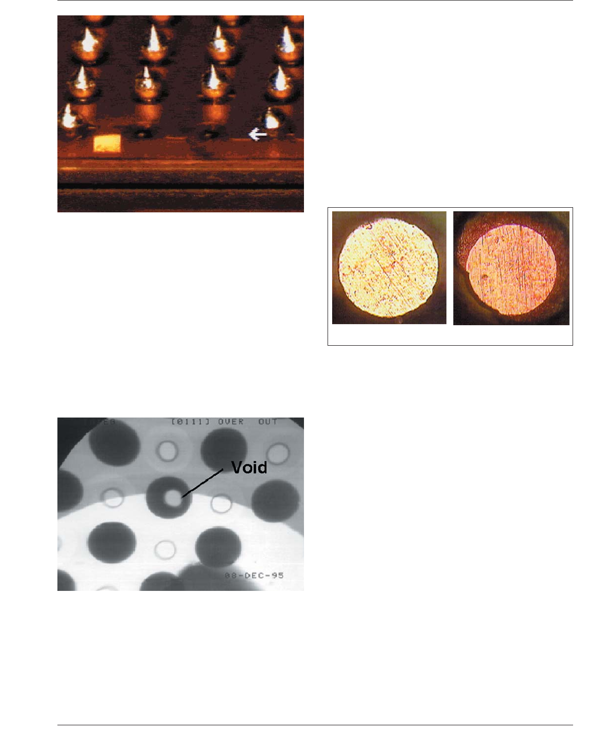
found in solder balls at incoming inspection indicate
reduced solder volumes in the solder balls. This will trans-
late to smaller collapsed solder ball stand-off heights and
thus may reduce reliability.
For voids found during post-assembly inspection, reliabil-
ity of the solder joint may be compromised if a void is
excessive due to the reduction of solder cross-section
and/or surface bonding area both at the interposer and the
product board. It will be necessary to establish an accept-
able level of voiding so that the product can meet customer
expectations, has a useful working life and meets product
reliability requirements.
4.8.3 Solder Ball Attach Integrity One of the factors the
success of the BGA package depends upon is reliable sol-
der ball attachment. The solder balls need to be attached
within acceptable dimensional tolerances. Their height and
width after attach need to be within specified and/or
acceptable limits. Most important of all, they need to form
a proper metallurgical bond with the lands on the substrate.
All the solder balls need to see a temperature profile which
ensures wetting necessary for optimum connection. If the
joint does not wet, then the solder ball is not properly
attached for necessary mechanical and electrical intercon-
nect. Such balls may fall off during shipping, transportation
and handling, or may fail or act intermittently during elec-
trical testing. Figure 4-29 shows the surfaces of the solder
ball and the land. The left picture shows the flattened bot-
tom of a solder ball and the right picture shows the pad on
an FBGA where a ball was supposed to be attached.
If the attach process temperature is inadequate to form a
proper metallurgical bond, only a small amount of force is
needed to dislodge the solder ball from the pad since it was
held in place only by mechanical adhesion.
Solder ball attach integrity can be evaluated through solder
ball shear. Manual and automated shearing and shear force
recording instruments are available for that purpose. For
shear test it is not only the magnitude of the shear force
that is important, but also the failure mode. Failures at the
solder interface, indicated by ripping soldering pads out of
the resin matrix of the BGA or the lands of the PCB, are
positive indications of good wetting. For good attachment,
there should not be any unwetted areas.
4.8.4 Package and Ball Coplanarity Package coplanar-
ity is the result of all of the following factors:
1. Package thickness, pitch, and thermal requirements
2. Substrate design, material, and manufacturing processes
3. Number of devices (silicon) - size and thickness
4. Number of passives - size and thickness
5. Assembly materials and manufacturing processes
Coplanarity that is currently specified at room temperature
does not always ensure that the component will have a
proper joint formation at SMT. The package behavior dur-
ing reflow (dynamic warpage) could result in good or bad
contact with the solder during reflow regardless of room
temperature coplanarity. The dynamic warpage of the pack-
age depends on the package CTE (package size, die size,
package material). The dynamic warpage signature could
Figure 4-27 Example of Missing Balls on a BGA
Component
Figure 4-28 Example of Voids in Eutectic Solder Balls at
Incoming Inspection
Figure 4-29 Examples of Solder Ball/Land Surface
Conditions
Flattened bottom of
a solder ball
Pad on an FBGA where it was
supposed to be attached
January 2013 IPC-7095C
35
Copyright IPC-Association Connecting Electronics Industries
Provided by IHS under license with IPC
Not for Resale
No reproduction or networking permitted without license from IHS
--`,,```,,,,````-`-`,,`,,`,`,,`---