IPC-7095C-2013.pdf - 第75页
Unless the via is filled or plated shut, then air is likely to remain under the solder paste forming a void in the solder ball when reflowed. For metal-defined lands with microvias, crack-propagation will start from the voi…
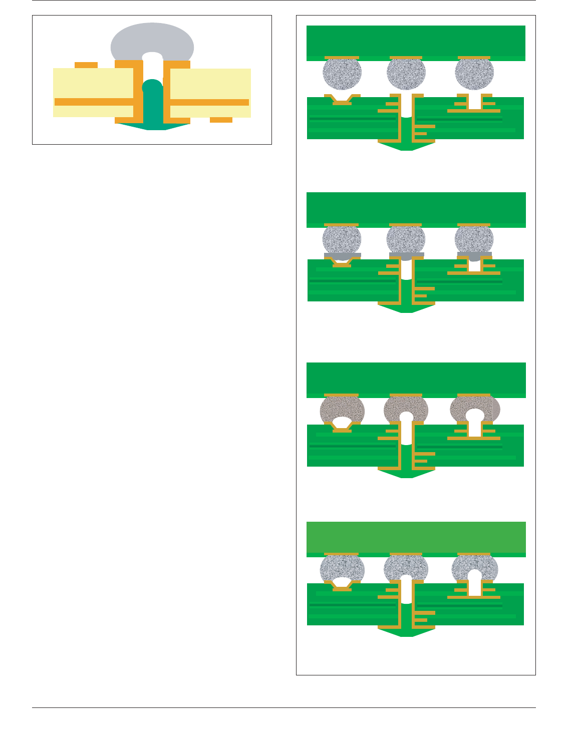
Vias capped on one side can pose a variety of reliability
issues. Each issue should be evaluated for relevancy to the
specific environmental design criteria:
• the hole may be partially filled creating uneven stresses
• the void may utilize a sizable part of the connection area
reducing the structural support
• the void may reduce the thermal path
When using via-in-pad technology, a void will occur in the
joint as shown in Figure 6-19, unless the via is capped on
the component placement side of the board. Most experts
agree that these void conditions, created due to entrapped
air, are acceptable and have no impact on the reliability of
the joint. There is no doubt that the conditions depend not
only on the process, but the size of the BGA land and the
diameter of the hole. In addition, there is a difference as to
whether the hole is a through-hole, blind via, or microvia.
Figure 6-20 shows the characteristics of the three hole con-
figurations and what takes place at incoming after the sol-
der paste has been printed and the BGA has been placed;
the conditions of the ball and hole during reflow soldering;
and, finally, the characteristics of the resulting solder joint.
One of the major reasons for the occurrence of the void
conditions is the entrapped gas that exists under the solder
paste during the original paste printing and BGA place-
ment. During the reflow operation, the entrapped gas and
the solder paste volatiles need to escape, and this creates
the minor occurrences of absence of solder at the center
part of the ball as shown in the illustration.
6.3.6 Fine Pitch BGA Microvia in Pad Strategies When
the pitch is less than 0.8 mm, there is not enough room to
place a via using current mechanical drill technology for
full array BGA components. For finer pitch BGAs, in order
to achieve increased routing area, putting a microvia-in-pad
may be necessary. These are blind vias that connect to the
first or second internal layer of the printed board. They are
typically laser drilled but, in some cases, a mechanical
drilling process is used (see Figure 6-21).
IPC-7095c-6-19
Figure 6-19 Cross Section of Via-in-Pad Design Showing
Via Cap and Solder Ball
IPC-7095c-6-20
Figure 6-20 Via-in-Pad Process Descriptions
BGA
Incoming - Before Assembly Process
During Reflow Soldering
Post Reflow Soldering
After Solder Paste
Printing & BGA Placement
IPC-7095C January 2013
60
Copyright IPC-Association Connecting Electronics Industries
Provided by IHS under license with IPC
Not for Resale
No reproduction or networking permitted without license from IHS
--`,,```,,,,````-`-`,,`,,`,`,,`---
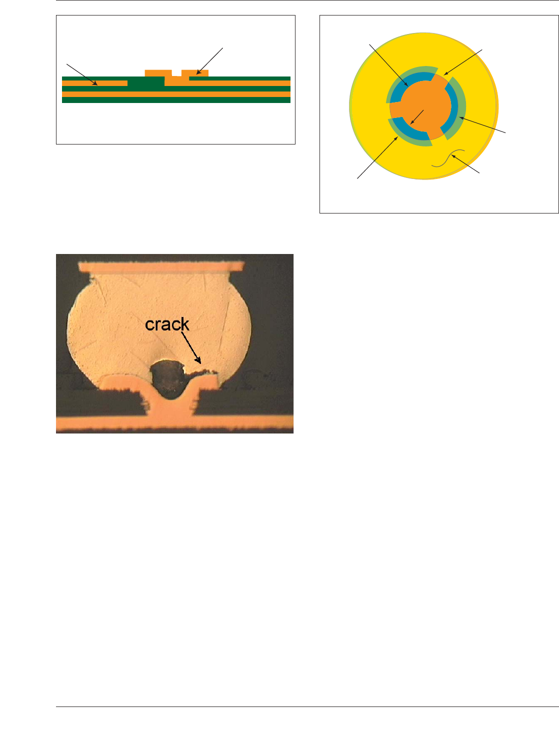
Unless the via is filled or plated shut, then air is likely to
remain under the solder paste forming a void in the solder
ball when reflowed. For metal-defined lands with
microvias, crack-propagation will start from the void asso-
ciated with the via and move towards the outside of the ball
(see Figure 6-22).
These voids have been shown to decrease the amount of
stress that the solder joint can withstand when compared to
a comparable MD land without via in pad. For this reason
it is not recommended to use via in pad for high stress sol-
der balls such as the corner balls or those directly under the
edges of the die.
6.3.7 Power and Ground Connectivity When lands are
required within a ground or power plane, it is a common
practice to leave an opening in the solder mask covering
the plane to provide access to the land. When increased
fatigue life is needed for these locations or for thermal iso-
lation, an MD land can be created within the plane etching
crescent-shaped relief pattern around the land (see Figure
6-23). Two, three, or four spokes (SMD Segments may be
used. The MD Segment should be arranged so that the
SMD segment is facing towards the corner of the BGA to
provide maximum fatigue strength.
6.4 Impact of Wave Solder on Top Side BGAs
6.4.1 Top Side Reflow
Mixed Technology printed circuit
boards are typically assembled by first reflow soldering the
surface mount packages on the top side of the board and
then wave soldering the through-hole packages (inserted
from the top side). For double-sided boards, the bottom
side SMT components are usually placed before top side
components and can be reflowed or adhesive used to hold
them in place. Bottom side components must be shielded
from the wave by a wave pallet if not secured with adhe-
sive. During the wave soldering process step, however, the
reflow soldered surface mount components on the top side
of the board are also heated. This heating can cause the
solder joints of these components to melt if the temperature
increases close to the liquidus point of the solder alloy.
Hence, care needs to be taken to prevent the solder joints
of these components from reaching the liquidus tempera-
ture.
6.4.2 Impact of Top Side Reflow BGA solder joints need
particular attention in this regard since the solder joints are
under stress during the wave soldering operation. If these
solder joints reach the liquidus temperature (183°C for the
eutectic tin/lead solder composition; 217°C for SAC alloy)
then there is a potential to de-wet or be pulled away from
the board or the package substrate due to the thermo-
mechanical strains induced in them at the elevated tem-
peratures. Since solder is extremely soft, even at tempera-
tures approaching the liquidus temperature, the potential
for cold solder, de-wetting or ball deformation exists when
their temperatures do not reach solidus.
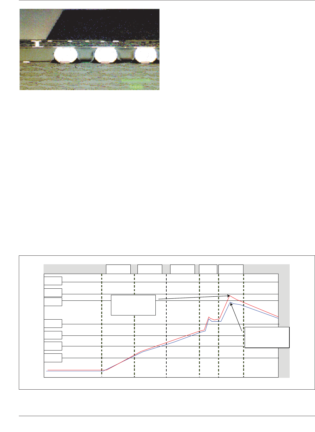
Figure 6-24 depicts examples of ball deformation and
de-wetting for a BGA component located on the top side of
a motherboard. The solder joints of the BGA reached a
peak temperature of 180°C during wave solder. BGAs are
more prone to such defects than leaded surface mount sol-
der joints since there is less strain relief.
IPC-7095c-6-21
Figure 6-21 Microvia Example
PCB pad
Cu layer
Cross-section
Figure 6-22 Microvia-in-Pad Voiding
IPC-7095c-6-23
Figure 6-23 Ground or Power BGA Connection
MD
Segment
Crescent Opening
Etched Into Plane
Copper Plane
Solder
Mask
SMD
Segment
January 2013 IPC-7095C
61
Copyright IPC-Association Connecting Electronics Industries
Provided by IHS under license with IPC
Not for Resale
No reproduction or networking permitted without license from IHS
--`,,```,,,,````-`-`,,`,,`,`,,`---
To avoid problems in BGA solder joints on the top side of
the board, their temperatures should not exceed 150°C dur-
ing tin/lead wave soldering and 190°C for lead-free alloy
wave soldering. This is less than the maximum temperature
allowed for the fine pitch leaded components such as plas-
tic QFPs.
Figure 6-25 is an example of an acceptable temperature
profile for the solder joints on a mixed technology board
during the wave solder process.
To determine the various ways of keeping the temperature
below 150°C (or 190°C for lead free), it is best to first
identify the various ways in which the BGA solder joints
are heated during the wave solder process. Figure 6-26
illustrated three pathways. Pathway A is by conduction
through the thickness of the board from bottom to top.
Pathway B is by conduction through the barrel of the via,
along a conductor connecting the via to the BGA solder
joint land. Pathway C is by convection and radiation from
the preheaters on the top in the wave solder machine.
6.4.3 Methods of Avoiding Top Side Reflow The meth-
ods of avoiding top side reflow aim to reduce the heat
transfer to the BGA solder joints by one or more of the
three pathways described above. Figure 6-27 illustrates
these methods. A heat shield can be placed over the BGA
packages to avoid direct heating from the preheaters in the
wave solder machine. These shields can be mechanically
attached to the wave solder pallets.
Secondly, vias can be capped by solder mask on the bottom
side of the board. This via-capping process is very com-
monly employed in the industry, for a variety of reasons.
Via capping rules should be built into the design for manu-
facturability (DfM) process, during board design.
Vias that certainly need to be capped are those that are
connected to the BGA land with a short trace length or
those that are connected to a plane in the board.
Thirdly, a nonmetallic wave shield can be placed immedi-
ately below the BGA package locations on the bottom side
of the board to avoid the wave from touching these board
locations. The wave shield can also be attached to the wave
pallet by nonmetallic fingers.
Selective wave pallets can utilize solid material under the
BGAs to prevent solder contact with the bottom of the
board and heat transfer up the vias to the lands. This will
prevent secondary reflow of the BGA joints.
The efficacy of each of these methods should be confirmed
by measuring the temperature profile of the BGA solder
joints during the wave solder process and ensuring that
they stay below 150°C.
Figure 6-24 Example of Top Side Reflow Joints
IPC-7095c-6-25
Figure 6-25 Example of Wave Solder Temperature Profile of Topside of Mixed Component Assembly
150° C
160° C
183°C
80° C
Zone # 2
100° C
Zone # 1 Zone # 3 Chip Contour
40° C
60° C
Maximum peak
temperature for
BGA is 150°
C
Maximum peak
temperature for
Fine Pitch is 160°C
IPC-7095C January 2013
62
Copyright IPC-Association Connecting Electronics Industries
Provided by IHS under license with IPC
Not for Resale
No reproduction or networking permitted without license from IHS
--`,,```,,,,````-`-`,,`,,`,`,,`---