IPC-7095C-2013.pdf - 第80页
reduces performance. It should also be noted that, using presently available testing concepts, maximum component I/O creates a condition that drives testing cost of the bare board dramatically higher due to multi-pass or…
To be damaging, the depressions have to be larger than
anticipated with current designs to entrap enough flux to
cause problems.
Some contacts are designed with individual force mecha-
nisms for each contact pin. Other contacts come with com-
mon force mechanism applied to all contacts simultane-
ously. All different kinds of contacting mechanisms will
leave some imprint on the solder balls. Contact size should
be matched with the solder ball size to be tested to mini-
mize the solder ball deformation. Therefore, the size of the
contact needs to decrease with decreasing solder ball sizes
and decreasing array pitches. Too large of a contact size
may short and may subject the solder ball to undesired lev-
els of deformation.
The force mechanism to assure contact needs to match the
solder ball hardness, which is dependent upon the solder
constituents. Too much force will impart unnecessary
deformation. The force mechanism needs to provide
enough force to contact the smallest balls in an array. The
solder balls soften when subjected or exposed to elevated
temperatures and time durations. Force mechanism design
needs to take this change in consideration for their use at
varying temperatures. Even at ambient, continuous testing
of parts may increase the temperature at the contact site.
For all practical purposes, the solder ball needs to be sol-
derable with acceptable contact strength, contact area and
solder column shape after it has endured the rigors of test-
ing and burn-in. To assess the impact of processing through
test and burn-in, the items to look at should include solder-
ability, coplanarity, and general cosmetic shape of the sol-
der ball. The solder ball should not lose so much solder to
the test and burn-in process that enough solder is not left
for optimum connection. The ball should be able to
respond to the reflow process to produce an acceptable
contact. Ball corrosion and foreign material picked up dur-
ing test and burn-in should not adversely affect the quality
and long-term reliability of the solder ball. After the test
and burn-in cycle, especially for no-melt balls, meeting the
coplanarity expectations will be an essential requirement
for proper BGA attachment to substrate.
Various technologies contact different parts of the solder
ball. In fact, most of the contact designs touch the bottom
of the solder ball to make a contact. In view of these
options, it would be impossible to declare certain parts of
the solder ball untouchable during its processing. To keep
a certain area of the solder ball untouchable is neither prac-
tical nor necessary if it has no effect on solderability, copla-
narity, solder volume, quality and reliability of the end
product.
6.5.3 Bare Board Testing There are a number of issues
that arise when considering the test inspection and mea-
surement of increasingly complex substrate interconnec-
tions, especially when involved with the electrical evalua-
tion of the substrate. In order for the manufacturer to be
able to reduce cost, while adequately assuring the electri-
cal function of the substrate interconnection, the customer
will have to provide definitive test data, with the preference
being 100% net list testing. Compatibility of the data is
currently an issue as well. It is hoped that industry stan-
dardization efforts will help to solve this issue in the fore-
seeable future. One item which could prove key to achiev-
ing this is likely to be acceptance of a standard base grid
pitch, which would allow test equipment and socket manu-
facturers to examine and focus on creation of a universal
solution.
The use of fixtures and bed of nails testing for opens and
shorts testing is quickly losing the ability to meet test
requirements as feature size decreases, coupled with
increased densities. Double density, or 1.77 mm pitch, test
beds seem to be adequate for 400 µm pitch and up. As the
density of the substrate increases beyond 400 µm pitch,
alternative techniques must be considered. Quad density
fixturing is a possibility, with 62 test probes per square
centimeter, but concern increases about potential feature
damage due to the contact by the probes. In addition, the
cost of double and quad density fixtures, as well as the cost
of test equipment, make it difficult to justify total test cov-
erage within cost expectations based on current understand-
ing of electrical testing and a linear projection of present
testing concepts.
Regarding the I/O density of 200 to 1000 at various grid
segmentation, it becomes apparent that double and quad
density is capable for bare board continuity testing the
average I/O requirements. However, if components are
stacked ‘‘edge-to-edge’’ the testing becomes impossible
with this test approach. This is because a BGA on 1.0 mm
pitch contains 96 lands per cm
2
, and the quad density test
fixture is only able to accommodate 62 probes per cm
2
.
Spreading components on the mounting structure relieves
some of that complexity but also consumes more space and
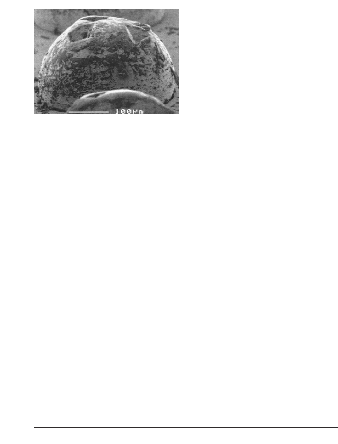
Figure 6-29 Pogo-Pin Type Electrical Contact Impressions
on the Bottom of a Solder Ball
January 2013 IPC-7095C
65
Copyright IPC-Association Connecting Electronics Industries
Provided by IHS under license with IPC
Not for Resale
No reproduction or networking permitted without license from IHS
--`,,```,,,,````-`-`,,`,,`,`,,`---
reduces performance. It should also be noted that, using
presently available testing concepts, maximum component
I/O creates a condition that drives testing cost of the bare
board dramatically higher due to multi-pass or dual fixture
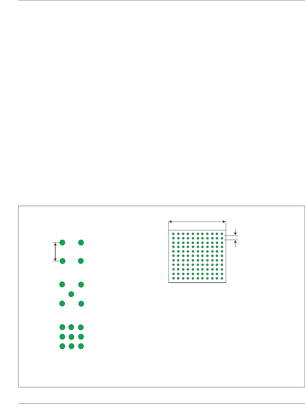
testing in order to have full test coverage. Figure 6-30
shows the relationship of part land requirements compared
to fixture capability.
Flying probe testing eliminates the need for costly fixtures
and, depending on the volume of substrates being manufac-
tured, can provide a cost-effective alternative to bed-of-
nails testing. The test is relatively slow depending on the
equipment used, and the equipment can be expensive. The
problem is compounded by the increased density require-
ments and the need for additional net testing. Most of this
equipment/test technique has evolved from the semicon-
ductor industry and has experienced some difficulty in scal-
ing to meet the mechanical challenges associated with
larger panel sizes. In addition, the small feature size in
some instances defeats the detection system due to the dif-
ficulties in charging the feature with the probe. Additional
equipment development will have to take place if technolo-
gies such as this are going to be useful for the complex
substrates of the future.
As via size continues to decrease, the limits of conven-
tional evaluation with metallographic microsection will
become less viable. 150 µm vias seem to be the practical
limit for microsection labs of average competence. An
alternative test method will be required if companies want
to know more about the plating in the via than just conti-
nuity. An electrical Interconnect Stress Test (IST) is pres-
ently being used by some companies to determining hole
integrity and reliability.
6.5.4 Assembly Testing Design of a printed board
assembly for testability normally involves system level
testability issues. In most applications, there are system
level fault isolation and recovery requirements such as
mean time to repair, percent up time, time to operate
through single faults, and maximum time to repair. To meet
the contractual requirements, the system design may
include testability features, and many times these same fea-
tures can be used to increase testability at the printed board
assembly level. The printed board assembly testability phi-
losophy also needs to be compatible with the overall inte-
grations, testing and maintenance plans for the contract.
The factory testers to be used, how integration and test is
planned, when printed board assemblies are conformal
coated, the depot and field test equipment capabilities and
personnel skill level are all factors that must be considered
when developing the printed board assembly test strategy.
The test philosophy may be different for different phases of
the program. For example, the first unit debug philosophy
may be much different than the test philosophy for spares
IPC-7095c-6-30
Figure 6-30 Area Array Land Pattern Testing
Double Density
Quad Density
100 TP/sq. in.
15.5 TP/sq. cm.
200 TP/sq. in.
31 TP/sq. cm.
400 TP/sq. in
62 TP/sq. cm.
0.10 in
P, mm. Z,cm I/O TP/sq. cm ET
1.5 2.53 300 46.9 QD
1.27 2.06 300 70.6 >QD
1.0 1.76 300 96.8 >QD
Z
Note: Fixture density assumes that components are minimum distance from each other
and ET pins from outside the package outline cannot be used. When components are
not brickwalled then pins can be gathered from outside the device land pattern.
Single Density
P
IPC-7095C January 2013
66
Copyright IPC-Association Connecting Electronics Industries
Provided by IHS under license with IPC
Not for Resale
No reproduction or networking permitted without license from IHS
--`,,```,,,,````-`-`,,`,,`,`,,`---

when all the systems have already been shipped. Before the
PWB design starts, requirements for the system testability
functions should be presented at the conceptual design
review. These requirements and any derived requirements
should be partitioned down to the various printed board
assemblies and documented. The system and program level
test criteria and how they are partitioned down to the
printed board assembly requirements are beyond the scope
of this document.
The two basic types of printed board assembly test are
functional test and in-circuit test. Functional testing is used
to test the electrical design functionality. Functional testers
access the board under test through the connector, test
points, or bed-of-nails. The board is functionally tested by
applying predetermined stimuli (vectors) at the printed
board assembly’s inputs while monitoring the printed board
assembly outputs to ensure that the design responds prop-
erly. In-circuit testing is used to find manufacturing defects
in printed board assemblies.
In-circuit testers access the board under test through the
use of a bed-of-nails fixture which makes contact with each
node on the printed board assembly. The printed board
assembly is tested by exercising all the parts on the board
individually. In-circuit testing places fewer restrictions on
the design. Conformal coated printed board assemblies and
many Surface Mount Technology (SMT) and mixed tech-
nology printed board assemblies present bed-of-nails
physical access problems which may prohibit the use of
in-circuit testing. Primary concerns for in-circuit test are
that the lands or pins (1) must be on grid (for compatibility
with the use of bed-of-nails fixture), and (2) should be
accessible from the bottom side (a.k.a. noncomponent or
solder side of through-hole technology boards) of the
printed board assembly.
Manufacturing Defects Analyzer (MDA) provides a low
cost alternative to the traditional in-circuit tester. Like the
in-circuit tester, the MDA examines the construction of the
printed board assembly for defects. It performs a subset of
the types of tests, mainly only tests for shorts and open
faults without power applied to the printed board assembly.
For high volume production with highly controlled manu-
facturing processes (i.e., Statistical Process Control tech-
niques), the MDA may have application as a viable part of
a printed board assembly test strategy. Vectorless Test is
another low cost alternative to in-circuit testing. Vectorless
Test performs testing for finding manufacturing process-
related pin faults for SMT boards and does not require pro-
gramming of test vectors. It is a powered-off measurement
technique consisting of three basic types of tests:
1. Analog Junction Test – DC current measurement test
on unique pin pairs of the printed board assembly
using the ESD protection diodes present on most
digital and mixed signal device pins.
2. RF Induction Test – Magnetic induction is used to test
for device faults utilizing the printed board assemblies
device protection diodes. This technique uses chip’s
power and ground pins to make measurements for
finding solder opens on device signal paths, broken
bond wires, and devices damaged by ESD. Parts incor-
rectly oriented can also be detected. Fixturing contain-
ing magnetic inducers are required for this type of test.
3. Capacitive Coupling Test – This technique uses
capacitive coupling to test for pin opens and does not
rely on internal device circuitry, but instead relies on
the presence of the metallic lead frame of the device to
test the pins. Connectors and sockets, lead frames and
correct polarity of capacitors can be tested using the
technique.
6.5.4.1 Board Flexure During Testing Since lead-free
joints can be stiffer and less ductile than tin/lead joints,
in-circuit/functional test fixtures can damage solder joints if
their design and manufacturing results in excessive board
flexing during use. This board flex induced damage is typi-
cally caused by improper location of board supports and
hold-downs, especially around areas with high concentra-
tions of test probes. Excessive board flexure may also be
caused by improper planar alignment of supports and hold-
downs, high probe forces, as well as by excessive or insuf-
ficient vacuum or improper distribution of springs between
top plate and probe plate. In addition, improperly designed
tooling and fixtures can easily lead to improper flexure of
the PCB, leading to damage.
In order to ensure that a test fixture does not cause damage
to printed circuit assemblies (PCAs), strain and strain-rate
must be measured on PCAs during use of the test fixture.
Measurements must be done at the corners of BGAs using
three element rectangular rosettes placed according to the
recommended gauge placement in IPC/JEDEC-9704.
Strains and strain-rates should be specified in a ‘‘strain
limit specification’’ defining actuation, test or release
requirements of the unit under test (UUT).
• The strain measurement system must simultaneously
sample all elements in each rosette (e1, e2, e3) in order
to properly measure and calculate all strain components
• The generally accepted strain limits for tin/lead PCAs is
600 µε, either principal or diagonal
• The generally accepted strain limits for lead-free PCAs is
450 µε, either principal or diagonal
• The generally accepted maximum strain rate is 30,000
µε/sec, either principal or diagonal
• Typical damage acceptance criteria is: No damage to
BGA solder joints detected using cross-section FA
method
January 2013 IPC-7095C
67
Copyright IPC-Association Connecting Electronics Industries
Provided by IHS under license with IPC
Not for Resale
No reproduction or networking permitted without license from IHS
--`,,```,,,,````-`-`,,`,,`,`,,`---