IPC-7095C-2013.pdf - 第31页
It is recommended that the user specify that plastic encased BGAs be furnished in the tray format rather than the tape- and-reel format. The tray carrier will accommodate the potential need to bake-out devices that are p…
Termination Cross-Section Before
Reflow Soldering on Board
Termination Cross-Section After
Reflow Soldering on Board Package Name
Solder Ball
Land
Solder
Mask
Package Substrate
Solder Joint
Board
Land
Solder
Mask
Package
Ball Grid Array (BGA)
Solder Bump
Package Substrate
Land
Solder
Mask
Solder Joint
Package
Land
Solder
Mask
Board
Solder Grid Array (SGA)
Package Substrate
High PB
Solder Ball
Fillet
Solder
Mask
Land
Solder Joint
Fillet
Package Substrate
Board
Land
Solder
Mask
Ceramic BGA (CBGA)
Socket Terminal
Solder Joint
Board
Socket Body
Land
Board
Fillet
Column
Ceramic Package
Ceramic Column Grid Array (CCGA)
Socket
Terminal
Stamped
Solder
Preform
Socket Body
Land
Fillet
Column
Ceramic Package Substrate
Solder Charge™ SMT
µPLR
Solder Mas
k
Package Substrate
Land
µPLR
Solder Mas
k
Package Substrate
Board
PILR™
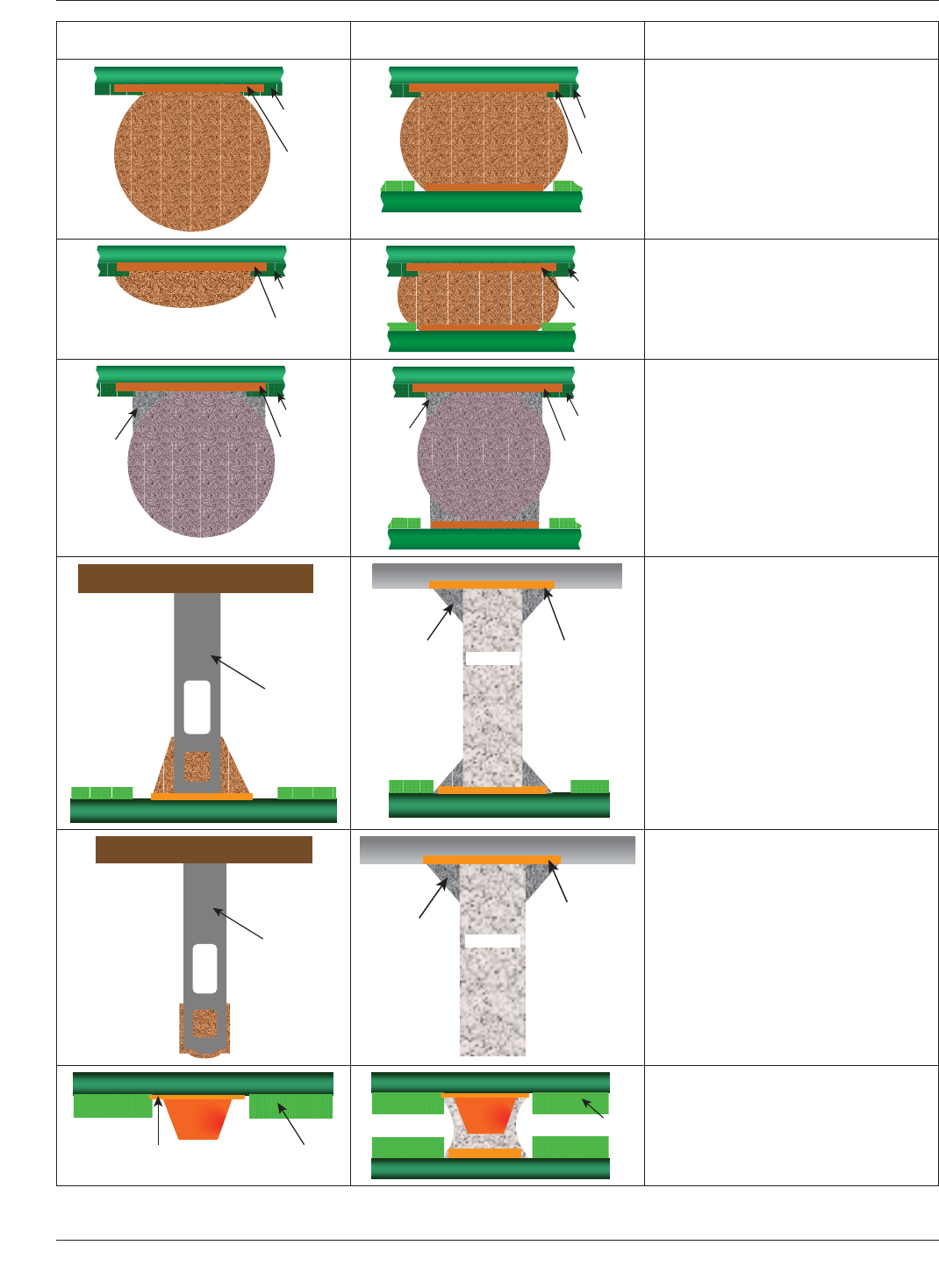
Figure 4-1 Termination Types for Area Array Packages
IPC-7095C January 2013
16
Copyright IPC-Association Connecting Electronics Industries
Provided by IHS under license with IPC
Not for Resale
No reproduction or networking permitted without license from IHS
--`,,```,,,,````-`-`,,`,,`,`,,`---

It is recommended that the user specify that plastic encased
BGAs be furnished in the tray format rather than the tape-
and-reel format. The tray carrier will accommodate the
potential need to bake-out devices that are prone to mois-
ture absorption. For example, if the plastic BGA packages
are exposed to ambient conditions beyond their floor life,
they will likely require baking before assembly. The plastic
tray carriers developed for bake-out are rated to withstand
125°C temperature. The tape-and-reel materials, on the
other-hand, cannot be exposed to temperatures above 50°C
without damaging the carrier tape. So baking a moisture-
sensitive BGA in the tape format could take many days.
4.1.5 Thermal Performance Thermal enhancements
have become essential with introduction of faster and faster
microprocessors. With introduction of new generations of
microprocessors, power dissipation has continually moved
upward. As the device clocking speed increases, the power
goes up. The problem of higher power is mitigated, fortu-
nately, with ‘‘die shrink’’ made possible by the reduction of
transistor feature sizes in contemporary semiconductor pro-
cesses and the associated trend towards lower power sup-
ply voltages. (As device geometry shrinks, the field inten-
sities increase, promoting a reduction in supply voltages to
avoid destructive effects.) The ceramic BGA is commonly
used for higher wattage packages, as it has greater thermal
conductivity than plastic packages. Plastic packages, how-
ever, have also evolved, and thermally enhanced plastic
packages are already in wide use by the industry. Ther-
mally enhanced plastic packages used to be limited to 6 to
8 watts; however, by incorporating integral metal heat
spreaders, plastic packages can accommodate up to 30
watts.
4.1.6 Real Estate Real estate constraint is one of the
important driving forces in reducing component package
size. This has contributed to the widespread usage of sur-
face mount devices, which are not only smaller in size, but
enable component mounting on both sides of the board. As
pin counts increase however, even with surface mount, the
conductor-to-conductor pitch must decrease to keep the
size of the package within a practical range for manufac-
turing.
As the contact pitch of the BGA package decreases, the
opportunity for placing more components in a given area
increases. Although the board real estate can now support
more functions per unit area, components such as the fine
pitch BGA (FBGA) will likely require more narrow con-
ductors and closer conductor spacing for interconnection.
For assemblies with very high component density, a greater
number of conductive layers may be needed to maintain a
smaller circuit board form factor.
4.1.7 Electrical Performance Electrical performance
drivers include signal integrity, operating frequency, power,
and pin-count. With increasing frequency, the need for
improved impedance control and minimal package inser-
tion loss is a concern. When impedance control require-
ments are imposed, one must consider the need for termi-
nations to prevent or dampen reflections. These
terminations, if performed in parallel to source and/or load
points on critical signals, will increase power consumption.
High frequency operation itself, all other things being
equal, drives power consumption upward with the square
of frequency. As such, low power semiconductor develop-
ment has increased in an attempt to reduce the average
power consumption of complex digital ICs. Fortunately, as
IC processes mature, the power per logic operation
decreases by virtue of smaller device feature sizes. In the
case of ceramic packages, even with increase in bond lands
for high-speed devices, the pin count growth required for
power and ground distribution is kept to a minimum by
exploiting the intrinsically high package capacitance and
employing package-mounted bypass capacitors.
4.1.8 Mechanical Performance The susceptibility of
BGA assemblies to other failure modes caused by mechani-
cal shock, vibration and/or bending should also be
assessed. Procedures described in IPC-9702, IPC-9703,
IPC-9704, IPC-9707 and IPC-9708 provide guidance in
completing assessments such as mechanical shock and
bend testing. The interconnect failure modes from these
type of exposures extend beyond solder joint failure. One
other failure mode that may be observed through this type
of mechanical testing is pad cratering, the fracturing of the
resin layer in the PCB under the BGA pad. These cracks
initiate at the edge of a BGA pad and continue to propagate
through the underlying resin layer. The fracture may follow
various paths. There may be an adhesive failure between
the copper pad and the underlying resin, or there may be a
cohesive failure due to a fracture entirely within the resin
layer.
Electrical failure will occur when the conductor trace lead-
ing to the BGA pad fractures. Depending on the location of
the mechanical loading, the trace fracture may occur either
before or after the pad crater fracture propagates under the
BGA pad. This phenomenon can result in the risk of latent
defects creating long term reliability exposure. A pad cra-
ter may be initiated during the mechanical handling of
assembly processing, but not detectable at test by electrical
failure. Subsequent thermo-mechanical exposure may
result in the propagation of the crack through a conductor,
and later, electrical failure in the field. Even if the conduc-
tor does not crack, the laminate crack creates the potential
for increased moisture ingress which could result in CAF
formation.
4.2 Die Mounting in the BGA Package There are many
ways a die is mounted in a BGA. The three main variations
can be differentiated by the medium of signal transmission
January 2013 IPC-7095C
17
Copyright IPC-Association Connecting Electronics Industries
Provided by IHS under license with IPC
Not for Resale
No reproduction or networking permitted without license from IHS
--`,,```,,,,````-`-`,,`,,`,`,,`---
from the die to the solder ball array. In the basic three
designs, the signal is carried by wire, conductive material
(flip chip) or conductive ribbon-lead. The substrate can be
ceramic or organic. The package properties will depend on
the properties of the substrate material and its dimensional
parameters. The following descriptions represent the more
common methodology for die-to-package assembly.
4.2.1 Wire Bond There are two main forms of the wire
bonded BGA. They are chip-on-board (COB) with the
active surface of the die facing away from the substrate,
and board-on-chip (BOC) types with the active surface of
the die facing toward the substrate. In both these structures,
the bond pads on the die are generally furnished at the
periphery and the wire bonds are made from the die periph-
ery to the lands on the substrate surrounding the die.
The die can be attached to the substrate using conductive
or nonconductive adhesive. Use of electrically conductive
adhesive is specified when the die backside requires an
electrical connection. The drawback is that the substrate
area under and equivalent to size of the die cannot be
accessed for in-package circuit routing. If the die does not
require a backside electrical connection, then a nonconduc-
tive adhesive can be used to place the die on the substrate.
In this case, the area under the die can be used for signal
routing.
The adhesive selected for die attach must not adversely
affect the mechanical integrity of the traces or the integrity
of the electrical signal. Following die attach and adhesive
curing process, the die is ready for electrical interface to
the substrate base. The bond pads on the die are connected
electrically to the bond pads on the substrate using gold
wire or aluminum wire where feasible. The traces on the
substrate route the signals from wire bond pads to the ball
grid array on the bottom of the substrate through plated via
holes. Following the wire-bond process, the die and bond
area is typically protected by encapsulation. Encapsulation
material can be applied in the form of glob top or it can be
molded in a press. An alternative to encapsulation is the
post-assembly attachment of a pre-molded cover.
In the BOC or die face-down structure, the bond pads on
the die can be located at the die periphery or in a row or
rows at the center of the die. The substrate is designed with
a narrow slot to accommodate the row or rows of bond
pads on the die. The die-to-substrate adhesive is placed to
the right and left of the bond pads. The adhesive can be
applied in the form of a paste or a film. The active or cir-
cuit side of the die is attached face-down onto the substrate
with the substrate slot exposing the bond pads on the die
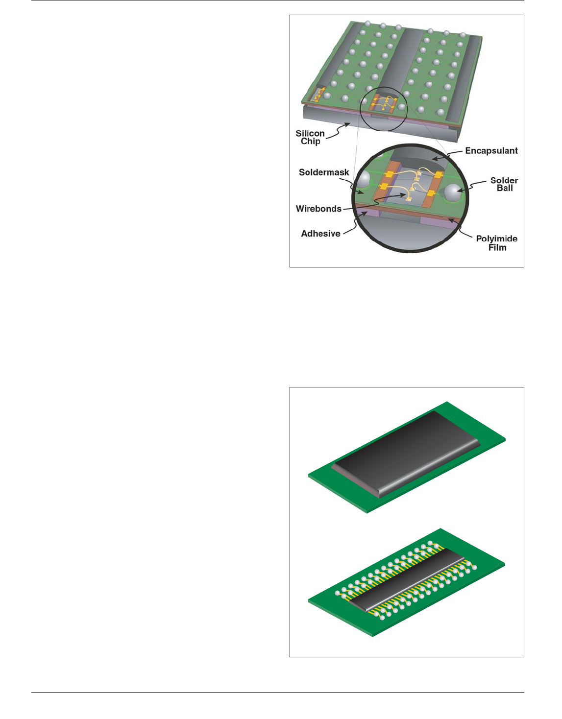
typical of that shown in Figure 4-2.
Following die attachment and adhesive cure, the bond pads
on the die are wire-bonded to the corresponding pads sur-
rounding the slot on the substrate. Following wire-bond,
the wires and exposed die surface are encapsulated for pro-
tection. Note that one or more grid array rows will need to
be depopulated to allow the slot in the substrate for wire
bond to the die. Also note that the wire bonding is accom-
plished at the center of the die and does not require
additional peripheral area around it for die-to-substrate
interface. Figure 4-3 illustrates the top and bottom of a
mold-encapsulated BGA package.
IPC-7095c-4-2
Figure 4-2 BOC BGA Construction
Top
Bottom
IPC-7095c-4-3
Figure 4-3 Top of Molded BOC Type BGA
IPC-7095C January 2013
18
Copyright IPC-Association Connecting Electronics Industries
Provided by IHS under license with IPC
Not for Resale
No reproduction or networking permitted without license from IHS
--`,,```,,,,````-`-`,,`,,`,`,,`---