IPC-7095C-2013.pdf - 第28页
fatigue damage caused by a CTE mismatch between the silicon die and interposer . Solder joint fatigue at the assembly level is mitigated when CTE mismatch is minimized and stand-of f height is increased. The reliability …
Standardization efforts were undertaken by many organiza-
tions such as JEDEC, IEC and IPC to test BGA packages
to the requirement limits of the bulk of the applications.
The majority of these plastic packages are going into office
equipment, laptop computers and portable electronic appli-
cations that do not require the life cycle performance
requirements needed by other applications.
Application-specific qualification standards are needed to
relate the test conditions to the environment in which the
product will be used. Many of the industry technology
roadmaps have identified these environments as being low-
cost benign, handheld, high-function handheld, cost perfor-
mance, high performance and harsh environments. The lat-
ter environments, such as those for Aerospace or
Automotive (under-the-hood) electronics, often require
additional testing such as highly accelerated stress testing
(HAST) in order to verify reliability in those harsh envi-
ronments.
Since pad cratering became an issue, IPC committees
developed a test procedure to attempt to qualify the printed
board before it is ever used as an assembly mounting struc-
ture, IPC-9708 provides test methods to evaluate the sus-
ceptibility of printed board assembly (PBA) materials and
designs to cohesive dielectric failure underneath surface
mount technology (SMT) attach pads. The test methods can
be used to rank order and compare different printed board
materials and design parameters, but do not define accep-
tance criteria.
3.5.10 Reliability Concerns Reliability concerns relate
to the BGA components themselves and to the reliability of
the BGA solder attachment to the interconnecting substrate,
usually an organic printed board.
Component reliability issues are mitigated through proper
mounting of the die to the interposer. Wire bonding tech-
niques have been used for many years. The processes
are well known, often times quite refined, and can afford
high yields. Another popular technique is to mount the bare
die face down onto the interposer in a flip chip configura-
tion. Using flip chip processes requires a tighter control
of the land positions on the interposer so that the lands line
up properly with the bonding sites on the bare die. In addi-
tion, if the interposer is made of organic materials, the
attachment process also requires underfill to minimize the
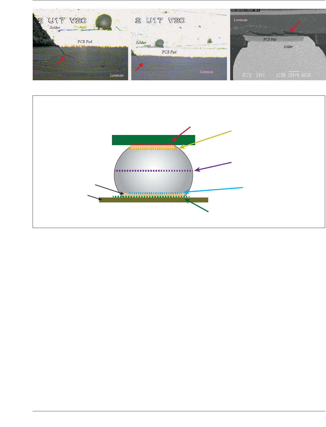
Figure 3-9 Examples of Pad Cratering
IPC-7095c-3-10
Figure 3-10 Various Possible Failure Modes for a BGA Solder Joint
Component Substrate
Land Pad
PCB
Failure between
component
substrate and
pad (Location 1)
Failure between
substrate pad and
ball (Location 2)
Failure within
solder, typically
seen in Post-
Thermocycle
(Location 3)
Failure between
ball and pad
(Location 4)
Failure between
pad and board (Pad
Cratering) (Location 5)
Solder Ball
January 2013 IPC-7095C
13
Copyright IPC-Association Connecting Electronics Industries
Provided by IHS under license with IPC
Not for Resale
No reproduction or networking permitted without license from IHS
--`,,```,,,,````-`-`,,`,,`,`,,`---

fatigue damage caused by a CTE mismatch between the
silicon die and interposer.
Solder joint fatigue at the assembly level is mitigated when
CTE mismatch is minimized and stand-off height is
increased. The reliability of the solder attachment can be
optimized by developing a thorough understanding of the
product’s operational use environment and by following
the guidance outline in the design for reliability (DfR) pro-
cedure suggested in IPC-D-279. Risk of tin whiskers and
gold embrittlement should be considered when selecting
surface finishes. Thick gold (more than 0.25 µm) as a sur-
face finish should be avoided to mitigate the risk of gold
embrittlement of the solder. Excessive thickness of other
noble metals as a surface finish should also be avoided.
3.5.11 Drivers for Lead-Free Technology There are two
drivers for corporations to convert their products from
those containing the ubiquitous tin/lead solder to a lead-
free solder. One is a legislative driver and the other is a
marketing driver.
The current legislative driver for eliminating lead in elec-
tronics and electrical equipment is the Restrictions on Haz-
ardous Substances (RoHS) Directive (2002/95SEC). The
RoHS Directive limits the percentage of lead, mercury,
cadmium, hexavalent chromium and two brominated flame
retardants that can be present in electrical and electronic
equipment that enters the market in the European Union
(EU). Currently there is no legislation in either the United
States or Japan that restricts the use of lead in electronic
products. There are requirements in Japan to recycle a lim-
ited number of used electronic equipment including PCs,
CRTs, TVs and White Goods. There is also an EU Direc-
tive on Waste in Electrical and Electronic Equipment
(WEEE). It requires that the waste be managed and
recycled according to the Directive which took effect in
2005.
The other driver is a marketing driver. Corporations are
developing and introducing lead-free products as a market-
ing initiative. Essentially, they do not want to be upstaged
by competitors who could introduce lead-free or halogen
free products before them. The BGA components, as well
as the entire electronic assembly must meet all of the leg-
islative and marketing criterion. Producers of electronic
products are required to provide declarations as to the
materials or substances contained in the products, thus this
requirement is moved down to the supply chain.
4 COMPONENT CONSIDERATIONS
4.1 Semiconductor Packaging Comparisons and Driv-
ers
There are many types of package formats for ICs but
only four types of terminal shapes: in-line pin (both single
and dual); pin grid array; J lead; and gull-wing lead. The
most common lead configurations for surface mountable
plastic packaged ICs are the J-lead and gull-wing lead. Of
these two, the gull-wing lead form is the most commonly
used lead type for plastic packaged ICs. One of the biggest
problems with higher pin count, fine-pitch gull wing leads
is their fragility, and consequently, susceptibility to lead
damage such as coplanarity, lead bending and sweep. Lead
damage is one of the leading causes of defects in fine-pitch,
gull wing leaded packages. Although gull wing devices are
the most commonly used lead form for low and high pin
count packages, ball grid array packaged devices have
achieved broad acceptance due to their physical robustness,
(pin-for-pin) size reduction and enhanced electrical perfor-
mance. In regard to performance, the BGA signal paths can
be much shorter than those of fine-pitch gull wing lead
packages, advantageous in high-speed applications. BGA
packaged ICs have exhibited very high board level assem-
bly process yields due to their ability to self-align during
reflow soldering. Because the array format can accommo-
date high I/O within a small form factor, BGAs have
proven to be a practical solution to the higher pin count
packaging trend as well.
4.1.1 Package Feature Comparisons The designs and
configurations of terminations for array area components
have evolved significantly in recent years from the simple
ball being attached to a land on the package substrate. The
Ball Grid Array (BGA) configuration is the most basic, and
still the most widely used termination design for area array
packages. A solder ball is reflow soldered onto the land of
a package substrate using either flux or solder paste. This
package, with balls on its underside, can then be subse-
quently reflow soldered onto boards using the standard
SMT soldering process. The solder balls melt fully and
collapse when forming the solder joint.
The Solder Grid Array (SGA) termination design dispenses
with the solder ball and just prints solder paste on the
package land. The resulting solder bump is then reflow sol-
dered onto boards to form the solder joint using the stan-
dard SMT soldering process. The drive for thinner product
designs has increased the use of SGA terminations in
recent years.
Making the interposer out of ceramic material is also a
technique used for producing grid array packages. The
Ceramic Ball Grid Array (CBGA) termination design is
similar to the BGA design but the ball used in this concept
does not melt fully and collapses during the board attach-
ment process. The composition of the ball is typically
90%Pb-10%Sn (High Pb). Due to the wide mismatch in
expansion between the ceramic substrate and the epoxy-
based board laminate, a high stand-off height needs to be
maintained for the solder joint to provide adequate reliabil-
ity. The noncollapsing high Pb solder ball provides this
requirement. The high lead ball has been replaced by a
lead-free alloy that also does not collapse.
IPC-7095C January 2013
14
Copyright IPC-Association Connecting Electronics Industries
Provided by IHS under license with IPC
Not for Resale
No reproduction or networking permitted without license from IHS
--`,,```,,,,````-`-`,,`,,`,`,,`---

In order to address the need to mount a ceramic package on
an organic printed board and accommodate the differences
in their respective CTEs, a column of solder provides the
attachment termination. The Ceramic Column Grid Array
(CCGA) termination design is an extension of the ceramic
ball grid array (CBGA) package. The CCGA uses a
90%Pb-10%Sn cast column instead of a high melt ball to
create a higher standoff and more flexible interconnection.
This achieves a significant increase in reliability. This high
lead alloy has also been supplanted by a lead-free alloy for
those applications that prohibit the use of lead as a sub-
stance in the final electronic product.
The SMT Solder Charge™ (SMT SC) termination design
was developed by a socket supplier to improve the solder
joint yield and reliability of area array socket terminations
when assembled on a printed board. This termination is a
stamped metallic pin which has the soldering element cut
from strip made from lead-free or tin/lead alloys. The sol-
der element itself extends beyond the end of the terminal.
As the solder melts, the solderable device as a whole is
lowered towards the PCB engaging solder points that were
previously more distant. Also, the malleable tip of the sol-
der element deforms when pushed into the PCB, again
compensating for coplanarity errors. Likewise, the protru-
sion on the end of the terminal can push through solder
paste to help compensate for coplanarity errors. When
reflowed, the SMT SC solder engulfs the stamped terminal
and adheres to the PCB’s solder land to form a bugle
shaped fillet. The exact shape of this fillet is controlled by
the size/shape of both the solder land and the wettable sur-
faces of the SMT SC terminal. These wettable surfaces of
the terminal are defined (i.e., limited) by a laser-ablated
zone which stops unwanted wetting, and so keeps the mol-
ten solder from ‘‘running up the terminal.’’
The Pillar (PILR™) termination is designed for very fine
pitch, chip-scale level packages and entails a small solid
copper contact feature in the package land. This design
enables a finer contact pitch array configuration, which in
turn provides a greater potential for increasing I/O density
and improved circuit routing efficiency. Furthermore, the
µPILR termination overcomes many of the existing limita-
tions of the spherical terminations. These include very
close contact spacing (<0.3 mm is possible), dramatically
lower package profile, enhanced electrical and thermal per-
formance, and ruggedness, exhibiting excellent physical
shock (drop) and vibration reliability results. Figure 4-1
shows the various area array termination designs that are
available today.
4.1.2 BGA Package Drivers The emphasis on faster,
smaller and lighter electronics systems is making compo-
nent, board, and system packaging more complex. The
increase in assembly complexity is due in part to the wide
use of small outline surface mountable packages, the key to
miniaturization of electronics products. The device contact
pitch plays a critical role in the complexity of manufactur-
ing processes as well. For example, with the adoption of
finer and finer contact pitches, greater precision is
demanded for each process in the assembly sequence: pick-
and-place, solder paste printing, and solder reflow. Inspec-
tion, rework and repair need to become more precise as
well.
Key issues to be addressed when selecting BGA compo-
nent packaging are thermal and electrical performance, real
estate constraint and cost. The component packaging
requirement varies for different types of systems. For
example, the high-end microprocessors run at higher fre-
quencies and require thermally and electrically enhanced
packages. Examples of thermal enhancements are heat
slugs, heat spreaders, heat sink and fin-fan (fan mounted on
heat sink), etc. Examples of electrical enhancements are
multilayer and higher pin-count packages and in-package
capacitance. Hermetic ceramic packages are generally used
for the in-package capacitance application. For mid-range
systems, performance is important as well, but so is cost
(not that cost is not important for high end systems).
4.1.3 Cost Issues Lead-frame packaged ICs have tradi-
tionally maintained a relatively low manufacturing cost.
This is due to the very high volume of products being
offered in a limited package configuration. This allows the
manufacturer to utilize common tooling and molding pro-
cesses for a diverse number of customer applications. The
array package format, on the other hand, is more often
designed and engineered for a specific product application.
The initial cost for packaging BGA devices with a pin
count of less than 200 will most likely be greater than
lead-frame packaging. This is due in part to the unique
single application substrate design and additional package
assembly process steps. Cost parity between lead frame
packaged ICs and the BGA package is generally reached
when the device requires 200 or more I/Os.
4.1.4 Component Handling BGAs can be furnished in a
carrier tray format or tape-and-reel. The EIA standard
embossed tape-and-reel format is often specified when the
IC components are relatively small and/or required for very
high-volume applications. The JEDEC registered carrier
trays are furnished to meet industry developed design
guidelines (see JEDEC publication 95, Section 4.9 and
Section 4.10) with a fixed length, width, and thickness. The
plastic packaged ICs, including the BGA, are susceptible to
moisture retention that can damage the package during
reflow solder processing. To protect the devices from
undue physical contact and exposure to humidity, the
loaded carrier trays are shipped in a sealed ESD and
vacuum purged moisture resistant envelope (and should
remain sealed until ready for board level assembly (see
4.8.5).
January 2013 IPC-7095C
15
Copyright IPC-Association Connecting Electronics Industries
Provided by IHS under license with IPC
Not for Resale
No reproduction or networking permitted without license from IHS
--`,,```,,,,````-`-`,,`,,`,`,,`---