IPC-7095C-2013.pdf - 第62页
damage the via wall resulting in open vias. However , applying the via caps after the surface finish has been applied can degrade some surface finishes (e.g., OSP , ImAg, ImSn) due to the thermal exposure that is necessary…

5.4.2 Photoimageable Solder Masks Photoimageable
solder masks provide accurate registration, are easy to
apply, encapsulate the circuit lines totally, have excellent
durability, and are cheaper than dry film.
Photoimageable masks can be either screened on or applied
by a process called curtain-coating in which the board is
passed at high speed through a curtain or waterfall of sol-
der mask.
The photoimageable mask may contain solvent along with
photopolymer liquid. If the solvent is added in the mask,
the liquid mask is screened on, solvent is dried off in an
oven, and then the mask is exposed to UV light by off-
contact or on-contact methods. (If no solvents are used, the
liquid is 100% reactive to UV light.) The off-contact
method requires a collimated light system to minimize dif-
fraction and scatter in liquid. This makes the system very
expensive. The on-contact approach needs no collimated
UV light source, and the system is relatively cheaper.
5.4.3 Jettable Solder Mask A new solder mask applica-
tion technology is becoming available to allow application
of solder mask in very fine pitch components. This technol-
ogy uses digital inkjet printer to print solder mask layer on
PCB or other substrates. The solder mask material is
applied directly on the substrate using digital data and set
of inkjet print heads with a resolution of 750 DPI.
The solder mask layer is implemented using one step as
opposed to using a four step process with the traditional
way of applying the solder mask. The solder mask material
is a specially-developed jettable ink. The ink is a solvent-
less hybrid system which is both UV and thermal curable.
Some of the advantages of the jetting system is the ability
to print narrow surface mount dams between fine-pitch
lands and tight control of the solder mask thickness. A few
disadvantages are that an end user must qualify the ink and
the material at the moment is only available in green color.
5.4.4 Registration of Board to Panel Image for Solder
Mask
Registration between individual boards within a
multi board panel becomes critical for any surface mount
application. This is especially true when the board is made
in a pallet format to assist the assembly process and
through-put characteristics. Board manufacturers inherently
build printed boards in a manufacturing panel format;
assemblers also want to take advantage of the multiple
board array format when they complete their assembly.
The positioning and orientation of individual boards on any
panel is usually at the discretion of the board manufacturer.
The manufacturer optimizes the use of the material in the
panel and the tolerance conditions that can be achieved
with the material used to build a particular board. It is a
well known fact that organic materials are prone to move-
ment (i.e. growth and/or shrinkage); thus, the board manu-
facturer, based on their knowledge of materials and their
predicted dimensional change movement, will commonly
adjust the photo tool of the circuit definition and the solder
mask definition to compensate for material stretch or
shrinkage depending on the circuit, the board size and the
particular properties of the selected solder mask material.
It is important to understand that assembly companies fre-
quently build their stencils based on a process of ‘‘step-
and-repeat’’ where elements of an individual board are
repeated to match the arrangement of the boards on the
subpanel. It is vital that the exact layout used by the board
manufacturer is understood to accurately provide the rela-
tionships of a land pattern for a BGA on one board with all
other land patterns of sister boards in the same panel.
Inconsistent arrangement of the assembly array can result
in misprints when stenciling solder paste onto the panel for
surface mount assembly.
5.4.5 Via Protection
5.4.5.1 Encroached vias
The encroached via concept is
one that permits solder mask being on the land without
filling the via plated-through hole. Encroachment vias take
the primary solder mask opening and adjust it so that it is
slightly larger than the via hole size.
This concept will permit any outgassing or cleaning of the
via plated-through hole, provide more surface coverage,
and increase adhesion between the solder mask and copper
of the annular ring. It will also provide a larger web
between the land and the via, and thus, should minimize
solder mask removal during BGA removal for rework.
5.4.5.2 Via Tenting, Plugging and Filling Via tenting,
plugging and filling (conductive or nonconductive) are
techniques used to cover or fill via holes with solder mask.
These processes serve different purposes. Via tenting, plug-
ging or filling is normally performed on boards that use
both reflow soldering and wave soldering. Via tenting,
plugging or filling is also recommended under certain
specified conditions, such as for boards where exposed vias
under BGAs are exposed to a wave solder. The concern is
based on the fact that, when a board with BGAs on the first
side is processed through wave soldering, a large amount
of heat can transfer from the vias. This can be very signifi-
cant because BGAs can have very high via densities
beneath them. The BGA’s joints can potentially reflow
again in the wave and a second reflow without flux could
result in cold solder joints or open joint conditions.
Via flooding and capping processing may be performed
after a surface finish has been applied. For OSP and ImAg
(immersion silver) finishes, via capping may be done after
the surface finish is applied because the harsh chemicals
that are used to clean the copper surface can become
trapped around the via cap. These trapped chemicals can
January 2013 IPC-7095C
47
Copyright IPC-Association Connecting Electronics Industries
Provided by IHS under license with IPC
Not for Resale
No reproduction or networking permitted without license from IHS
--`,,```,,,,````-`-`,,`,,`,`,,`---

damage the via wall resulting in open vias. However,
applying the via caps after the surface finish has been
applied can degrade some surface finishes (e.g., OSP,
ImAg, ImSn) due to the thermal exposure that is necessary
to cure the via cap material. Both of these issues must be
taken into account when making a decision to flood or cap
vias. Most PCB suppliers flood or cap vias before the sur-
face finish is applied.
There are presently eight different methods of via plugging/
capping identified in IPC standardization. These are shown
in Figure 5-12. It is important to realize that the choice of
tented, plugged and filled vias for via protection can have
direct impacts on the subsequent assembly processes.
Table 5-4 provides the pros and cons of tenting, plugging
and filling vias. The choice among the options presented
will depend on the capabilities of both the fabricators and
the assemblers. To avoid complication during assembly, it
is imperative that all involved in the manufacturing process
understand the trade-offs among the options.
5.5 Thermal Spreader Structure Incorporation (e.g.,
Metal Core Boards)
When structural, thermal, or electri-
cal requirements dictate, a conductive constraining core or
metal core can be inserted into the layer structure. It is rec-
ommended that the board circuitry layer configuration is
made symmetrical about the the core as the center. It is
possible to create structures that are asymmetrical (i.e.,
having a different number of layers to either side of the
core); however, plated-through holes going through the
entire stack may be less reliable due to the differences in
expansion on either side of the metal or constraining core
(see Figure 5-13).
One reason for asymmetrical design is the separation of
electrical functions from mechanical or thermal functions,
but this advantage might be offset by board distortion or
warping during soldering operations (or during thermal
cycling in the intended operating environment) due to dif-
ferences in the thermal expansion of materials.
Some compensation can be achieved by having additional
copper planes added to the back of the interconnection
product. The extra copper plane may increase the expan-
sion coefficient slightly and make soldering more difficult
due to the need to put more energy into the board to assure
proper solder joint formation; however, a positive effect is
that it enhances thermal conductivity.
5.5.1 Lamination Sequences As previously noted, more
desirable constructions are those where circuit layers are
symmetrical about the core chosen to serve at the center of
the board. By so doing, individual multilayer circuits can
be produced separately, each with their own laminating
sequence. For example, a four layer board might be manu-
factured having vias through the entire four layers and this
can be duplicated for use on either side of the core.
To achieve mechanical constraint within a chosen and use-
ful range, the total thickness of the core in the multilayer
should be approximately 25% of the board’s total thick-
ness. Constraining core board is more often used because
the core layers may be imaged, etched, and connected to
the plated-through hole. The thicker center core must be
machined. Better thermal cycle survival has been shown in
some studies for structures having two constraining cores
in the board rather than one.
Another configuration is to have a special constraining core
board made by bonding a multilayer board to each side of
a thick metal core after each of the boards has been com-
pleted. The composite board is then sequentially drilled,
plated, and etched to form plated-through hole connections
between the two boards. Coupons should be provided to
test the integrity of the composite structure.
5.5.2 Heat Transfer Pathway Metal core boards add sig-
nificantly to the thermal mass of the assembly. This may
force the preheating soldering process to be operated at
abnormally high limits. These designs should be thor-
oughly evaluated under production conditions prior to
release. Laminate ruptures and discoloration and grainier
textured solder are typical effects that have been observed.
The heat transfer path between components and the planes
are usually accomplished through either direct contact with
the plane or through thermal vias positioned under the
component and connected to the thermal core or plane in
its position.
Table 5-3 Via Filling/Encroachment to Surface Finish Process Evaluation
Surface Finish Tenting Flooding Capping Plugging Encroaching
HASL Okay Okay Okay Okay Okay
OSP Okay Not Recommended Okay Okay Okay
ENIG Okay Okay Okay Okay Okay
ImAg Okay Not Recommended Okay Okay Okay
ImSn Okay Not Recommended Okay Okay Okay
IPC-7095C January 2013
48
Copyright IPC-Association Connecting Electronics Industries
Provided by IHS under license with IPC
Not for Resale
No reproduction or networking permitted without license from IHS
--`,,```,,,,````-`-`,,`,,`,`,,`---
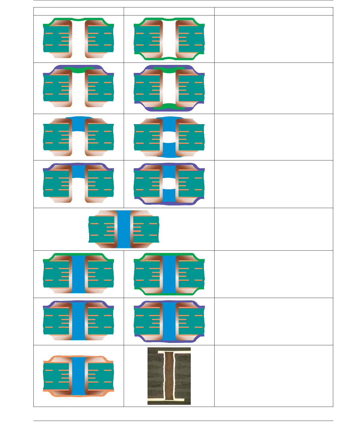
One side Type a Two sides Type b
Tented Via (Type I Via)
A via with a dry film mask material applied
bridging over the via wherein no additional
materials are in the hole. It may be applied
to one side.
(Type I-a) or both sides (Type I-b) of the via
structure (IPC-4761, Figure 5-1).
Tented and Covered Via (Type II Via)
A Type I via with a secondary covering of mask
material applied over the tented via. The material
may be applied to one side (Type II-a) or both
sides (Type II-b) of the via structure (IPC-4761,
Figure 5-2).
Plugged Via (Type III Via)
A via with material applied allowing partial
penetration into the via. The plug material
may be applied from either one side (Type III-a)
or both sides (Type III-b) of the via structure
(IPC-4761, Figure 5-3).
Plugged and Covered Via (Type IV Via)
A Type III via with a secondary covering of
material applied over the via. The plug and
secondary covering material may be applied
from either one side (Type IV-a) or both sides
(Type IV-b) of the via structure (IPC-4761,
Figure 5-4).
Filled Via (Type V Via)
A via with material applied into the via targeting
a full penetration and encapsulation of the hole
(IPC-4761, Figure 5-5).
Filled and Covered Via (Type VI Via)
A Type V via with a secondary covering of
material (liquid or dry film soldermask) applied
over the via. The covering material may be
applied from either one side (Type VI-a) or
both sides (Type VI-b) of the via structure
(IPC-4761, Figure 5-6).
Filled and Capped Via (Type VII Via)
A Type V via with a secondary metallized
coating covering the via. The metallization
is on both sides (IPC-4761, Figure 5-7).
Partially Filled Via
The illustrations show a via filled with
nonconductive epoxy and then plated
over with copper. This is commonly
used for via in pad applications
(IPC-4761, Figure 5-8).
Figure 5-12 Via Plug Methods
January 2013 IPC-7095C
49
Copyright IPC-Association Connecting Electronics Industries
Provided by IHS under license with IPC
Not for Resale
No reproduction or networking permitted without license from IHS
--`,,```,,,,````-`-`,,`,,`,`,,`---