IPC-7095C-2013.pdf - 第151页
T able 8-6 Accelerated T esting for End Use Environments Worst-Case Use Environment Accelerated T esting Use Category Tmin °C Tmax °C Δ T (1) °C t D hrs Cycles/ Y ear T ypical Y ears of Service Approx. Accept. Failure Ri…

solder joint reliability testing. There are multiple models
available and people use this to estimate the Pb-free solder
joint reliability, for their products and applications. There is
no universal agreement since these model are product-
specific.
The validation and qualification tests should follow the
guidelines given in IPC-SM-785, Guidelines for Acceler-
ated Reliability Testing of Surface Mount Solder Attach-
ments. However, for large components with significant heat
dissipation, for components of asymmetric construction,
and for small global CTE-mismatches, temperature cycling
tests are inadequate to provide the required information;
full functional cycling including external temperature and
internal power cycling is necessary.
8.8 Screening Procedures
8.8.1 Solder Joint Defects
The solder joint defects of
greatest reliability concern are those involving inadequate
wetting for whatever reason. Properly wetted solder joints
have adequate strength even for severe mechanical loading
conditions, without diminishing thermal fatigue resistance.
However, solder joints not properly wetted, can prema-
turely fail both as the result of mechanical and thermal
cyclic loading.
Voids in the solder joints are generally regarded as not
constituting a reliability threat. Possible exceptions are
large voids reducing the solder joint cross-section enough
to reduce a required thermal heat transfer function, and
voids in high-frequency applications where the voids can
cause signal deterioration.
BGA components having noncollapsible balls (high tem-
perature solder 90% Pb 10% Sn, with a melting point of
302°C) typically will have few or no induced voids
because the ball solder never melts during the reflow pro-
file.
8.8.2 Screening Recommendations Effective screening
procedures need to be capable of causing the failure of
latent solder joint defects, i.e., weak inadequately wetted
solder joints, without causing significant damage to high
quality solder joints. The best recommendation is random
vibration (6-10 grams for 10-20 minutes), preferably at low
temperature, e.g., -40°C. This loading does not damage
good solder joints, but overstresses weakly bonded ones.
Thermal shock can also be successfully used; however,
some damage to good solder joints can be expected, par-
ticularly for larger components.
8.9 Accelerated Reliability Testing The validation and
qualification tests should follow the guidelines given in
IPC-SM-785, Guidelines for Accelerated Reliability Test-
ing of Surface Mount Solder Attachments and/or IPC-9701,
Performance Test Methods and Qualification Requirements
for Surface Mount Solder Attachments. Although acceler-
ated temperature cycling (ATC) is often conducted, for
some products, ATC needs to be combined with mechani-
cal shock and/or vibration testing. From a single set of ATC
test conditions or inadequate ATC test conditions may not
provide valid conclusions.
Accelerated reliability testing is carried out on design pro-
totypes, typically to failure or until a predetermined reli-
ability goal is achieved. The appropriate reliability goal can
be determined with an appropriate acceleration model (see
IPC-D-279 Design Guidelines for Reliable Surface Mount
Technology Printed Board Assemblies).
Once failure occurs, the resulting failure modes are ana-
lyzed as to the underlying failure mechanism(s). If it fails
expectations then corrective action is necessary. Either the
assembly process needs to be improved or the product
needs to be redesigned. In either case retesting may be
necessary after the corrective action has been implemented.
Recognizing that a matrix was needed to determine the
exact requirements and the testing necessary for perfor-
mance under various conditions, the IPC Product Reliabil-
ity Committee developed the following table, ‘‘Product
Categories and Use Environments.’’ Table 8-6 attempts to
relate seven product categories by typical application to the
thermal, mechanical, atmospheric, and electrical perfor-
mance requirements that they must meet during typical
manufacturing processes, storage, and during operation.
IPC-7095C January 2013
136
Copyright IPC-Association Connecting Electronics Industries
Provided by IHS under license with IPC
Not for Resale
No reproduction or networking permitted without license from IHS
--`,,```,,,,````-`-`,,`,,`,`,,`---

Table 8-6 Accelerated Testing for End Use Environments
Worst-Case Use Environment Accelerated Testing
Use Category
Tmin
°C Tmax °C
ΔT
(1)
°C
t
D
hrs
Cycles/
Year
Typical
Years
of
Service
Approx.
Accept.
Failure
Risk %
Tmin
°C Tmax °C
ΔT
(2)
°C
t
D
min
1) Consumer 0 +60 35 12 365 1-3 1 +25 +100 75 15
2) Computers +15 +60 20 2 1460 5 0,1 +25 +100 75 15
3) Telecom -40 +85 35 12 365 7-20 0,01 0 +100 100 15
4) Commercial
Aircraft
-55 +95 20 12 365 20 0,001 0 +100 100 15
5) Industrial &
Automotive
Passenger
Compartment
-55 +95 20
&40
&60
&80
12
12
12
12
185
100
60
20
10 0,1 0 +100 100 15
& COLD
(3)
6) Military
Ground &
Ship
-55 +95 40
&60
12
12
100
265
10 0,1 0 +100 100 15
& COLD
(3)
7) Space
leo
geo
-55 +95 3
to 100
1
12
8760
365
5-30 0,001 0 +100 100 15
& COLD
(3)
8) Military
Avionics
a
b
c
-55 +95 40
60
80
&20
2
2
2
1
365
365
365
365
10 0,01 0 +100 100 15
& COLD
(3)
9) Automotive
Under Hood
-55 +125 60
&100
&140
1
1
2
1000
300
40
5 0,1 0 +100 100 15
& COLD
(3)
&
LARGE ΔT
(4)
& = in addition
1)
ΔT represents the maximum temperature swing but does not include power dissipation effects; for power dissipation calculate ΔT; power dissipation can make
pure temperature cycling accelerated testing significantly inaccurate. It should be noted that the cyclic temperature range, ΔT is not the difference between
the possible minimum, T
min
and maximum, T
max
, operational temperature extremes; ΔT is typically significantly less.
2)
All accelerated test cycles shall have temperature ramps, 20°C/minute and dwell times at temperature extremes shall be 15 minutes measured on the test
boards. This will give ~24 test cycles/day.
3)
The failure/damage mechanism for solder changes at lower temperature; for assemblies seeing significant cold environment operations, additional ‘‘COLD’’
cycling, from perhaps -40 to 0°C, with dwell times long enough for temperature equilibration and for a number of cycles equal to the ‘‘COLD’’ °C operational
cycles in actual use is recommended.
4)
The failure/damage mechanism for solder is different for large cyclic temperature swings traversing the stress-to-strain -20 to +20°C transition region; for
assemblies seeing such cycles in operation, additional appropriate ‘‘LARGE ΔT’’ testing with cycles similar in nature and number to actual use is
recommended.
January 2013 IPC-7095C
137
Copyright IPC-Association Connecting Electronics Industries
Provided by IHS under license with IPC
Not for Resale
No reproduction or networking permitted without license from IHS
--`,,```,,,,````-`-`,,`,,`,`,,`---
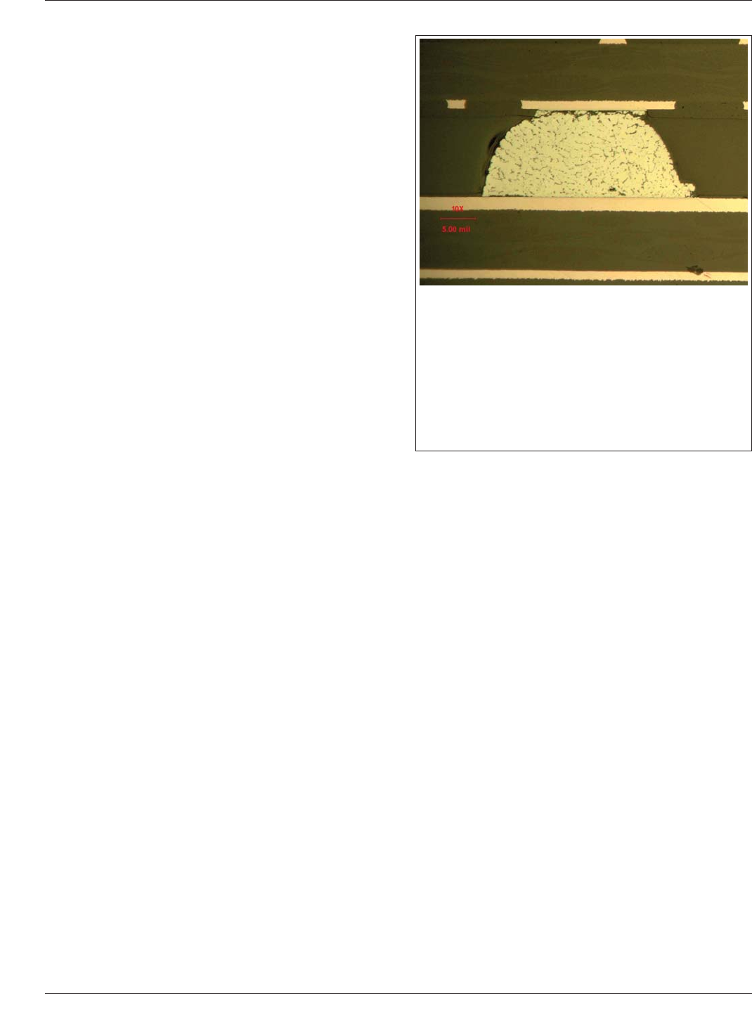
9 DEFECT AND FAILURE ANALYSIS CASE STUDIES
The following clauses identify possible assembly anoma-
lies related to the assembly of BGA components. The
descriptions include post process failures related to the
mounting structure characteristics and the variation in the
solder ball used as the BGA termination. In many instances
attachment metallurgy are discussed especially if the char-
acteristics contributed to the joint failure. Final joint con-
figurations are also analyzed.
9.1 Solder Mask Defined BGA Conditions There are
two ways BGA Lands are defined: solder masked defined
(SMD) where the land size is larger than solder mask and
the molten BGA ball touches the solder mask after reflow.
The other method for designing the BGA land is called
etched or nonsolder mask defined (NSMD) where the mask
opening is larger than the copper land and hence the ball
does not touch the solder mask after reflow. This condition
is shown in 9.1.1 and 9.1.2.
Solder mask-defined lands may be used on corresponding
noncritical or functional pins, since SMD lands can help
minimize pad cratering defects. However, it should be
understood that solder mask defined lands create additional
stress initiation sites and should be avoided on both the
interposer and the printed board land.
9.1.1 Solder Mask Defined and Nondefined Lands
Possible Cause
Interposer is solder mask defined; board is metal-defined. If the
two areas are very different, the stresses are not uniform and
cracks may occur at the solder mask defined side. Board land
pattern too large.
Potential Solution
Area of the two attachment conditions should be similar or
identical. In addition, solder mask defined lands create addi-
tional stress initiation sites and should be avoided on both the
interposer and the printed board land.
IPC-7095C January 2013
138
Copyright IPC-Association Connecting Electronics Industries
Provided by IHS under license with IPC
Not for Resale
No reproduction or networking permitted without license from IHS
--`,,```,,,,````-`-`,,`,,`,`,,`---