IPC-7095C-2013.pdf - 第90页
7 ASSEMBLY OF BGAS ON PRINTED CIRCUIT BOARDS 7.1 SMT Assembly Processes The assembly processes for attaching BGA components are more forgiving than the processes for attaching fine pitch peripheral components in some aspe…

the processes, and the shop-floor equipment. Applications
receiving messages from the equipment include:
• Work-in-process (WIP)
• Tracking, capacity, and throughput monitors
• Equipment utilization and line-balancing monitors
• Product quality monitors that incorporated data from test
and inspection
Linking all parts of a manufacturing operation through a
single hub has been the goal for many years. The CAMX
message-broker approach provides an extraordinary array
of tools to accomplish that task. The message broker can
connect any number of clients together. Clients can be fac-
tory equipment, a host computer, or the data hub at the
engineering manager’s desk. The system provides visual
representation of whatever the manager wants to know. The
manager can communicate with someone in Singapore, and
check the status of their work-in-process using a snapshot
of the data in any of a number of preset formats. He can
pick the format and instruct the software as to how fre-
quently the updates are required, and the broker does the
rest.
6.8.2.2 Information Exchange Benefits Major equip-
ment manufacturers have involved themselves in this effort
from the beginning, thus they support the CAMX effort to
extract information from their machines in the standard
format. Critical to the success of this new tool is its ‘‘plug-
and-play’’ construction. Any piece of equipment on the
floor can connect to the supporting architecture and data-
gathering software. Using XML as the standard ensures
that no one will misinterpret what the data means. Process
correction and product improvement require traceability of
faults, regardless of where a fault is identified. Knowing
where the fault came from and its root cause are critical.
In addition, increasing product quality and reducing costs
require understanding the actual fault spectrum. Histori-
cally, the same fault may be called by several names at dif-
ferent process points. Applying the CAMX standard, fault
names can be consistent from step to step within the manu-
facturing operation, thereby improving the overall level of
communication.
For electronics manufacturing service (EMS) providers, the
CAMX standards permit manufacturing flexibility without
sacrificing data coherence and comprehensive data analy-
sis, regardless of the process under evaluation. The soft-
ware is more streamlined and less complex than systems
that were developed for the semiconductor industry
because all of the equipment now conforms to the single
standard. The result is equipment that is both easier to use
and easier to support.
Standardization will open up opportunities to perform more
elaborate data analysis because the standards will reduce
the effort required to gather information. IPC-2501, as
implemented in the CAMX message broker, provides the
simplified web-based XML messaging activity for the other
IPC standard vocabularies. Equipment suppliers who need
a particular piece of information will merely ‘‘subscribe’’
to an application or system using the existing Web-based
and universal XML messaging SOAP protocol, regardless
of the architecture of the other interfaces, and download
responses in real time. SOAP is an XML messaging stan-
dard supported by all major computing and software
vendors. It forms the foundation of their Web-services
infrastructures.
The XML message type of machine communication was
less necessary when OEMs did their own manufacturing.
However, with the amount of outsourcing that kind of ver-
tical integration has become more the exception than the
rule. The new standards will make it possible for the OEM
customer to regain a measure of the insight into manufac-
turing activity that was lost due to outsourcing the work.
The use of a universal data format will also provide the
ability of suppliers to monitor inventory of their products
to prevent disruptions of the manufacturing line. Compo-
nent suppliers can monitor usage of their components on
the factory floor, scheduling purchases and taking over
similar functions that otherwise fall to the EMS company
or to the OEM.
6.8.3 Specifications In many instances, documentation
references other specifications. These should be clear and
should be provided in this same manner in which the origi-
nal package is provided (hard copy or electronic). Confor-
mance test circuitry shall be provided, thus the part can be
tested through destructive techniques. As a minimum, con-
formance test circuitry shall include:
• Board part number/revision letter
• Assembly part number and reference to Bill of Material
• Traceability identification
• Date code
• Manufacturer’s identification, e.g., commercial and gov-
ernment entity (CAGE), logo, etc.
• Special coding systems may be used provided they are
identified on the master drawing
January 2013 IPC-7095C
75
Copyright IPC-Association Connecting Electronics Industries
Provided by IHS under license with IPC
Not for Resale
No reproduction or networking permitted without license from IHS
--`,,```,,,,````-`-`,,`,,`,`,,`---

7 ASSEMBLY OF BGAS ON PRINTED CIRCUIT BOARDS
7.1 SMT Assembly Processes
The assembly processes
for attaching BGA components are more forgiving than the
processes for attaching fine pitch peripheral components in
some aspects, but more demanding in others. Process
defect rates are significantly less than fine pitch peripheral
components; however, good process control is a necessity.
7.1.1 Solder Paste and Its Application The surface
mount assembly process uses solder paste to connect the
BGA balls to the lands on the board. Solder paste can be
applied to the lands using three methods: screening, sten-
ciling, and dispensing. BGAs are typically printed using
stenciling where solder paste is applied on the BGA lands
through the apertures on the stencil of similar size or
smaller to the BGA lands.
Stencil thickness and aperture size will determine the
designed paste volume, which can be critical for the solder
joint reliability of certain BGA types. Squeegee type and
process settings will impact the actual solder paste that is
deposited. The stencil thickness may need to be reduced
when using finer pitch BGA components; however, care
needs to be taken when reducing stencil thickness so that
volume is not reduced for other components. Trapezoidal
stencil apertures (slightly larger opening on the bottom
than on the top) are generally preferred as they improve
paste release.
Solder paste consists of a homogeneous mixture of metal
powder particles and flux. The metal content (typically
90% by weight) in the solder paste determines the amount
of solder in the solder joint. The most common solder paste
alloy is the eutectic Sn63Pb37, and SAC 305 for lead-free
(Sn96.5Ag3.0Cu0.5). Metal powder particles are generally
spherical in shape. A uniform shape aids the printing or
dispensing process and it decreases the surface area, which
minimizes oxidation.
Flux makes up the majority of the remaining substances in
the solder paste. The activators in the flux remove oxides
from the solder particles, the land, and the BGA balls. They
promote good solderability during reflow process. Solder
balls, which form for a variety of reasons during reflow, are
a reliability concern, especially when fine pitch devices are
involved. The solvents have an important role in control-
ling the tackiness of the paste and affecting the rheological
properties. The formation of voids in the BGA solder joint
may be related to solvents in the solder paste. Solvents
with low boiling points and/or improper reflow parameters
can increase the incidence of voids in BGA solder joints.
For successful fine pitch BGA printing, the solder paste
must pass through very small apertures in the stencil. The
solder paste needs to remain printable and tacky for an
extended period of time, and it must maintain print defini-
tion prior to and during reflow. Solder paste viscosity, par-
ticle size and stencil life are critical parameters for solder
paste application.
7.1.1.1 Particle Size and Paste Selection Many solder
pastes are available and one should be selected based on
(among other things) the print characteristics, flux type,
and fine pitch particle size. Print characteristics includes
that the solder paste print well, providing good print defi-
nition without exhibiting solder paste slump. The flux in
the paste should be active enough to exhibit good wetting
and reflow characteristics, yet it should be compatible with
the cleaning process or surface resistivity requirements if a
no-clean flux is used. The diameter of the particle size
should not exceed the aperture width divided by 4.2. This
was determined through empirical experimentation. When
this rule is violated, the paste release and print definitions
are affected.
The solder particle size is classified by J-STD-005 (see
Table 7-1).
Particle size distribution affects the solder paste viscosity
and printability. Type 3 paste is the most commonly used,
and it is adequate for most printing applications. Ultra fine
pitch CSP application may require Type 4 paste. Care
should be taken when moving to Type 4 powder as the sol-
derability is generally reduced due to the increase in the
surface area and the potential for increased oxidation of the
solder particles. It is often necessary to use nitrogen in the
reflow furnace when Type 4 powders are incorporated.
7.1.1.2 Stencil Thickness and Aperture Design As is
the case for all components, as the pitch of the part
decreases it often becomes necessary to decrease the sten-
cil thickness. For BGA components in the pitch range of
1.5 mm to 1.0 mm, a stencil can range from 0.15 mm
[0.006 in] to 0.18 mm [0.007 in] thick. For chip scale
packages (CSP) or fine pitch BGAs with a pitch ≤0.80 mm,
a stencil thickness range of 0.1 mm [0.004 in] to 0.15
[0.006 in] mm is recommended. CSPs and other fine pitch
area array packages are seldom the only components on a
PCA so a balance must be struck in the selection of stencil
thickness. Thin stencils, appropriate for optimal CSP print-
ing, will likely not provide sufficient solder paste for other,
larger pitch BGAs. This can lead to defects such as head-
in-pillow or reduce the thermal fatigue life of critical
ASICs.
Table 7-1 Particle Size Comparisons
Solder Paste Type Mesh
Maximum Particle
Size [µm]
Type 2 -200/+325 75
Type 3 -325/+500 53
Type 4 -400/+500 38
Type 5 -500 25
IPC-7095C January 2013
76
Copyright IPC-Association Connecting Electronics Industries
Provided by IHS under license with IPC
Not for Resale
No reproduction or networking permitted without license from IHS
--`,,```,,,,````-`-`,,`,,`,`,,`---
When making decisions about stencil thickness and volume
of paste to be deposited, it is safer to deposit more paste
than less paste with the goal of achieving six times more
bridges than opens (this is the ratio and not more defects).
The reasons are that bridges can rarely escape inspection
and they are sure to be caught by tests (ICT or functional).
Opens and intermittent opens, on the other hand, can easily
escape tests since they may make contact due to pressure
applied during testing but will result in field failures. So
this simple guideline to target more bridges than opens
while designing stencil and land patterns is the most cost
effective method to prevent field failures.
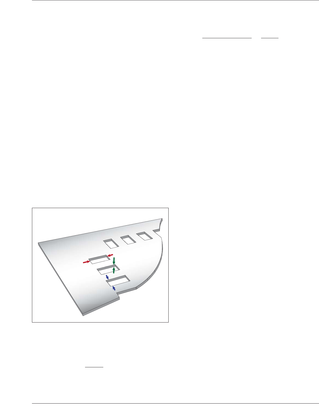
It is also very important to design a stencil aperture that
will provide good paste release. In order to ensure good
paste release, an aspect ratio of 1.5 is recommended.
Aspect ratio is the ratio between stencil aperture width and
stencil thickness. Another commonly used ratio is called
area ratio. An area ratio of greater than 0.66 is recom-
mended. The formula to calculate area aspect ratio is the
area of the stencil aperture divided by the area of the sten-
cil walls (see Figure 7-1). The idea behind designing sten-
cil with these strongly recommended aspect and area ratios
is to allow more paste release and minimize any paste
along the stencil walls which may partially clog apertures
and reduce paste volume on subsequent boards to be
printed next, resulting in insufficient solder joints or even
opens.
Area land contact/area stencil wall equals aperture/area of
aperture walls) = L*W/2*(L+W)*T >0.66
LxW
2(L+W)
xT
Note: Aspect ratio is more common than area ratio in
aperture design since aspect ratio is one dimensional sim-
plification of the area ratio when land length is much
greater than width i.e., a square aperture with a dimension
of 0.35 mm with a stencil thickness of 0.125 mm gives the
resulting aspect ratio:
0.35x0.35
2(0.35+0.35)x0.125
=
0.1225
0.175
= 0.70
Using an overprint or an aperture larger than the land may
be necessary to achieve this ratio, especially for finer pitch
BGAs, Stencil apertures are generally one to one or slightly
smaller than the land in order to achieve gasketing. When
and if the stencil apertures need to be larger than the lands,
to achieve the desired area ratio for better paste release,
cleaning of the stencil after each print may be necessary.
Larger apertures will cause paste to leak under the stencil
resulting in paste smudging on boards to be printed next. It
should also be noted that stencil apertures are significantly
larger than the lands when designing stencils for CBGAs,
CCGAs, and paste-in-hole processes.
A square or rectangular aperture with rounded corners will
also provide better paste release and volume deposition.
7.1.1.3 Importance of Paste Volume For plastic BGAs
much of their solder volume is supplied by the solder ball
on the part itself and the paste volume is not that critical.
For plastic BGAs (in both SnPb and lead-free configura-
tions) above 0.80 mm pitch, stencil thickness will be dic-
tated by the other component types used on the printed
board assembly. Solder volume and stencil thickness
become more critical for ceramic BGAs with noncollaps-
ible copper balls or high temp 90%Pb/10%Sn balls with
melting point of 302°C The solder balls used on ceramic
BGAs do not collapse during the normal reflow process
(see Figure 7-2).
For CBGA with noncollapsible balls (copper balls or 90Pb/
10Sn) where thicker solder volume is required, a stepped
stencil may be used. The step is typically 0.04 mm to
0.08 mm, and it can put two different paste thicknesses on
the board surface. A metal squeegee can be used success-
fully when the step is 0.04 mm. If a stepped stencil is used,
the step line should be at least 3.75 mm away from any
print aperture. Because the high lead content ball does not
collapse, having sufficient solder paste is critical. So in
addition to using stepped stencil, the stencil aperture may
also have to be much bigger than the land to achieve the
required paste volume for noncollapsible balls. The fillet
between the land and ball depend upon the solder paste
volume. Ceramic BGAs and CGAs require a minimum vol-
ume of solder pastes to make a reliable solder joint. There
are various suppliers of this type of technology who can
provide the specific solder paste volume for their package.
Table 7-2 contains an example of the solder paste volume
requirements for some of the ceramic packages using either
tin/lead or lead free (SAC) solder paste (see Table 7.2).
The paste volume requirements should be the same for
both tin/lead and lead free paste. Also the paste volume
IPC-7095c-7-1
Figure 7-1 Aspect and Area Ratios for Complete Paste
Release
Solder Stencil Feature Dimensions
Aperture length (L)
Stencil thickness (T)
Aperture width (W)
January 2013 IPC-7095C
77
Copyright IPC-Association Connecting Electronics Industries
Provided by IHS under license with IPC
Not for Resale
No reproduction or networking permitted without license from IHS
--`,,```,,,,````-`-`,,`,,`,`,,`---