IPC-7095C-2013.pdf - 第24页
BGA issues are not insurmountable; however , they require dedicated engineering resources to develop and implement a consistently reliable process. 3.5.1 Visual Inspection BGA is not a package suitable for companies that…

3.1.5 Inspection Requirements As with any surface
mount part, BGAs should not be moved after component
placement because this may smear the paste and cause sol-
der bridges. Even if some misalignment is visually
observed, many parts will self-align during reflow if their
terminations are no more than 50% off the land. If a BGA
has a gross misalignment problem, it should be removed
before reflow and reworked later. Though it may not be
practical for high volume production, using X-ray or opti-
cal inspection (endoscope) to inspect failures before
removing the part may be desirable.
3.1.6 Test Test strategies need to be developed before
using BGAs. The solder joints cannot be probed and test
points are required. It may be difficult to incorporate
enough test points to adequately test all solder joints. Some
alternative test strategies may be needed such as designing
BGA components with boundary scan capability designed
into them reducing the number of I/O fanout probe points.
In an effort to improve test capability, some BGA compo-
nents had test points designed right on the top of the pack-
age. This was not a good solution since it put pressure on
the BGA components and the joints.
3.2 Time-to-Market Readiness Before implementing
BGAs into products, it is important to address not just the
technical issues, but also the possible business implica-
tions. It is very likely that time-to-market will be adversely
impacted if both products and the technology are devel-
oped simultaneously. It is a good idea to first develop and
validate the technology before implementing it on a real
product. Otherwise, if any problem develops in the product
or technology, the deadline for product shipment will be
missed. To assure time-to-market readiness, BGA imple-
mentation methodology and process steps should be ana-
lyzed.
3.3 Methodology Several factors must be considered
when making design decisions in an attempt to balance
size, cost, and functionality. In addition to these consider-
ations, the product must also be able to perform reliably
over the expected lifespan of the product in its intended
environment. Package selection may be influenced by these
reliability factors and environmental conditions such as
temperature vibration, shock, and humidity.
3.4 Process Step Analysis There are several available
paths to utilizing BGAs effectively. The length of each path
depends on what design and assembly facilities a company
presently has, and how quickly they can be made ready for
production. The following is an example of one approach:
1. Select a list of candidate products for BGAs.
2. Develop an equipment list based on the projected vol-
ume needs. If sufficient in-house expertise does not
exist, it may be desirable to use a reputable training
center or consultant to save cost and time.
3. Organize a team representing design, production, test,
quality, and purchasing. This team is responsible for
component and equipment selections and review.
4. Develop a comprehensive BGA design guide that
stresses manufacturability. Use existing standards where
possible.
5. Design the candidate products starting with the conver-
sions of existing products using fine pitch components.
6. Determine the need for lead-free products including the
alloy used on the part as well as the surface finish
needed on the mounting substrate.
7. Conduct rigorous assembly and test reviews. Carefully
monitor component purchasing to assure that compo-
nents have the specified package, shipping method, met-
allization, solderability, and orientation in the shipping
containers.
8. Develop comprehensive workmanship standards and a
process control system that is statistically sound.
9. Design the remaining candidate products.
With the major emphasis on using parts that meet both
customer requirements and conform to new environmental
regulations, many customers are requiring reports listing all
materials used at the component level and also for com-
pleted assemblies. To help facilitate this, IPC has devel-
oped IPC-1751 and IPC-1752 on Materials Declaration,
and have encouraged software providers to make tools
available that meet the requirements of those standards.
The requirement to establish a formal declaration system
has been in place since the automotive industry was chal-
lenged by the ‘‘End-of-Life’’ European directives.
To show an example of the breadth of the variation in
material properties that may occur in products, Table 3-3
shows a list of materials that might be used as a surface
finish or a material that was added to the assembly as the
second level interconnection.
3.5 BGA Limitations and Issues Even though BGA tech-
nology has moved into the mainstream, there are still some
decisions that need to be considered. These are business
and technical issues that must be resolved. The areas of
special concern are:
• Visual inspection
• Moisture sensitivity
• Rework
• Cost
• Availability
• Voids in BGA
• Open joint (BGA or PoP BGA)
• Head-on-pillow phenomenon
• Standards and their adoption
• Reliability concerns
January 2013 IPC-7095C
9
Copyright IPC-Association Connecting Electronics Industries
Provided by IHS under license with IPC
Not for Resale
No reproduction or networking permitted without license from IHS
--`,,```,,,,````-`-`,,`,,`,`,,`---

BGA issues are not insurmountable; however, they require
dedicated engineering resources to develop and implement
a consistently reliable process.
3.5.1 Visual Inspection BGA is not a package suitable
for companies that assure quality by inspection and repair.
BGA solder joints cannot be inspected unless X-ray or
optical inspection techniques are used. To reap the benefits
that BGA offers, robust process control must be main-
tained. Due to limited time and training, many companies
find implementing such tight process control to be a diffi-
cult endeavor.
There are some visual inspections of BGAs that can iden-
tify problems with solder joints. These would show good
flow on an uncollapsed ball with ceramic BGAs, and also
be able to show collapsed balls on plastic BGAs on the
outer rows of the BGA. Visual inspection of the outer rows
serves as an indicator of some of these problems. Examples
are BGA alignment with the lands on the outer rows, and
how the BGA is sitting on the board, level or skewed.
3.5.2 Moisture Sensitivity The plastic BGA packages
are very moisture sensitive. This makes them susceptible to
warpage, swelling, popcorning, or cracking if the packages
are not properly baked and kept dry prior to package
assembly. Component storage and handling procedures are
critical for any moisture sensitive component including
leaded surface mounted devices, but it is critical for BGAs/
FBGAs.
Component moisture sensitivity is tested using J-STD-020
and is determined according to the package thickness. The
moisture sensitivity level must be analyzed for each BGA
package type. It is critical to know at which of the appli-
cable temperatures, 220°C, 235°C, 245°C, 250°C, or
260°C the BGA package was classified. The classification
of the package type may drop several levels if the higher
temperature is used.
Due to improvements in molding compounds and laminate
systems, most laminate-based BGAs can be mounted and
qualified for temperatures above 220°C. The hermetic
ceramic BGAs are not moisture sensitive and therefore can
be mounted using either of the higher temperatures.
Because of the switch to lead-free solders, the industry
needs to test and verify at a higher temperature such as
260°C, which will create major issues with not only BGAs,
but also all surface mounted devices.
3.5.3 Thermally Unbalanced BGA Design The plastic
BGA package is also susceptible to warpage at which time
the package edges lift up; this could result in no connec-
tions on the outer rows. The edges may also bend down,
Table 3-3 Potential Plating or Component Termination Material Properties
Gold (Au)
Gold (Au), electroplated
Gold (Au), hard
Indium (In)
Nickel/Gold (Ni/Au) ENIG
Nickel/Gold (Ni/Au), electrolytic
Nickel/Gold (Ni/Au),
Nickel/Palladium (Ni/Pd)
Nickel/Palladium/Gold (Ni/Pd/Au)
Nickel/Palladium/Gold (Ni/Pd/Au), ENEPIG
Organic Solderability Preservative (OSP)
Organic Solderability Preservative (OSP-HT), high temp
Palladium (Pd)
Platinum/Palladium/Silver (Pt/Pd/Ag)
Silver (Ag)
Silver (Ag), electroplated
Silver (Ag), immersion
Silver (Ag), with Nickel (Ni) barrier
Silver/Palladium (Ag/Pd))
Silver/Palladium (Ag/Pd), with Nickel (Ni) barrier
Tin (Sn)
Tin (Sn), bright
Tin (Sn), bright, annealed
Tin (Sn), bright, fused
Tin (Sn), bright, reflowed
Tin (Sn), bright, reflowed over Nickel (Ni) barrier
Tin (Sn), bright, with Nickel (Ni) barrier
Tin (Sn), bright, with Silver (Ag) barrier
Tin (Sn), hot dipped
Tin (Sn), immersion
Tin (Sn), matte
Tin (Sn), matte, annealed
Tin (Sn), matte, fused
Tin (Sn), matte, reflowed
Tin (Sn), matte, reflowed over Nickel (Ni) barrier
Tin (Sn), matte, with Nickel (Ni) barrier
Tin (Sn), matte, with Silver (Ag) barrier
Tin (Sn), reflowed
Tin (Sn), Semi-matte (Sn)
Tin/Bismuth (SnBi), <5% Bi
Tin/Bismuth (SnBi), =>5% Bi
Tin/Bismuth/Gold (Sn/Bi/Au)
Tin/Copper (Sn/Cu)
Tin/Copper (Sn/Cu), annealed
Tin/Copper (Sn/Cu), HASL
Tin/Copper (Sn/Cu), hot dipped
Tin/Copper (Sn/Cu) matte
Tin/Lead (Sn63Pb37)
Tin/Lead (Sn90Pb05)
Tin/Lead/Silver (Sn/Pb/Ag)
Tin/Silver (Sn/Ag)
Tin/Silver (Sn/Ag), hot dipped
Tin/Silver (Sn/Ag), plated
Tin/Silver/Bismuth (Sn/Ag/Bi)
Tin/Silver/Bismuth/Copper (Sn/Ag/Bi/Cu)
Tin/Silver/Copper (Sn/Ag/Cu)
Tin/Silver/Copper (Sn/Ag/Cu), hot dipped
Tin/Zinc (Sn/Zn)
Tin/Zinc/Aluminum (Sn/Zn/Al)
Tin/Zinc/Nickel (Sn/Zn/Ni)
NAC* (Not applicable - Must provide Comment)
IPC-7095C January 2013
10
Copyright IPC-Association Connecting Electronics Industries
Provided by IHS under license with IPC
Not for Resale
No reproduction or networking permitted without license from IHS
--`,,```,,,,````-`-`,,`,,`,`,,`---
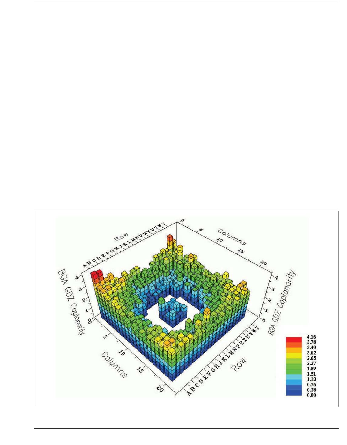
thus such terms as ‘‘frowning’’ or ‘‘smiling’’ BGAs have
been used to identify these conditions. The so-called ‘‘smil-
ing’’ BGA interposer puts a stress on the balls at the outer
rows, while the ‘‘frowning’’ BGA interposer puts the stress
on the connection of the inner row ball locations. Package
warpage is of real concern in flux-only applications during
rework. Large die sizes can cause CTE mismatch between
the PCB and the package laminate material, which can cre-
ate package warpage (see Figure 3-8).
Thermally unbalanced package designs, particularly those
with heat spreaders on the top, will warp according to the
classic bi-metal effect.
3.5.4 Rework Although BGAs do not require nearly as
much rework as fine pitch lead-frame devices, many
assemblers are apprehensive about using a component
package that is difficult to be reworked. While BGA rework
is difficult, it is by no means impossible. Tools and tech-
niques for rework are currently available that range from
manual to automated techniques to reball the BGA or
redress the land pattern. Several factors must be addressed
during the rework operation. These are:
• Number of heat cycles
• Ball collapse during re-balling
• No damage to pads on BGA interposer
• Proper land redressing and no damage to lands on the
product board
• Appropriate reflow temperature for re-attachment based
on alloy used
• Proper cleaning to remove flux residue unless no-clean
flux is used
3.5.5 Cost The BGA still has a slight cost differential
compared to fine pitch peripheral packages that it replaces.
However, competitive pressures keep bringing costs lower
to meet new targets. Further costs accrue with the increased
board layer counts that BGAs require; however, there are
many advantages to the interconnecting concepts and the
performance characteristics resulting from BGA implemen-
tation.
Following are some of the key reasons for higher BGA
package cost:
• Higher cost substrate (fine line/space)
• High T
g
BT (bismaleimide-triazine) resin
• Thermal enhancements
• Electrical enhancements
• Very fine external pitches
• High temperature reflow requirements
• Thin profile heights
IPC-7095c-3-8
Figure 3-8 BGA Warpage
January 2013 IPC-7095C
11
Copyright IPC-Association Connecting Electronics Industries
Provided by IHS under license with IPC
Not for Resale
No reproduction or networking permitted without license from IHS
--`,,```,,,,````-`-`,,`,,`,`,,`---