IPC-7095C-2013.pdf - 第118页
Whenever voids are observed in solder joints, they first need to be identified in one of the above categories, in order to determine their impact on joint reliability and to assess corrective actions to minimize or elimina…
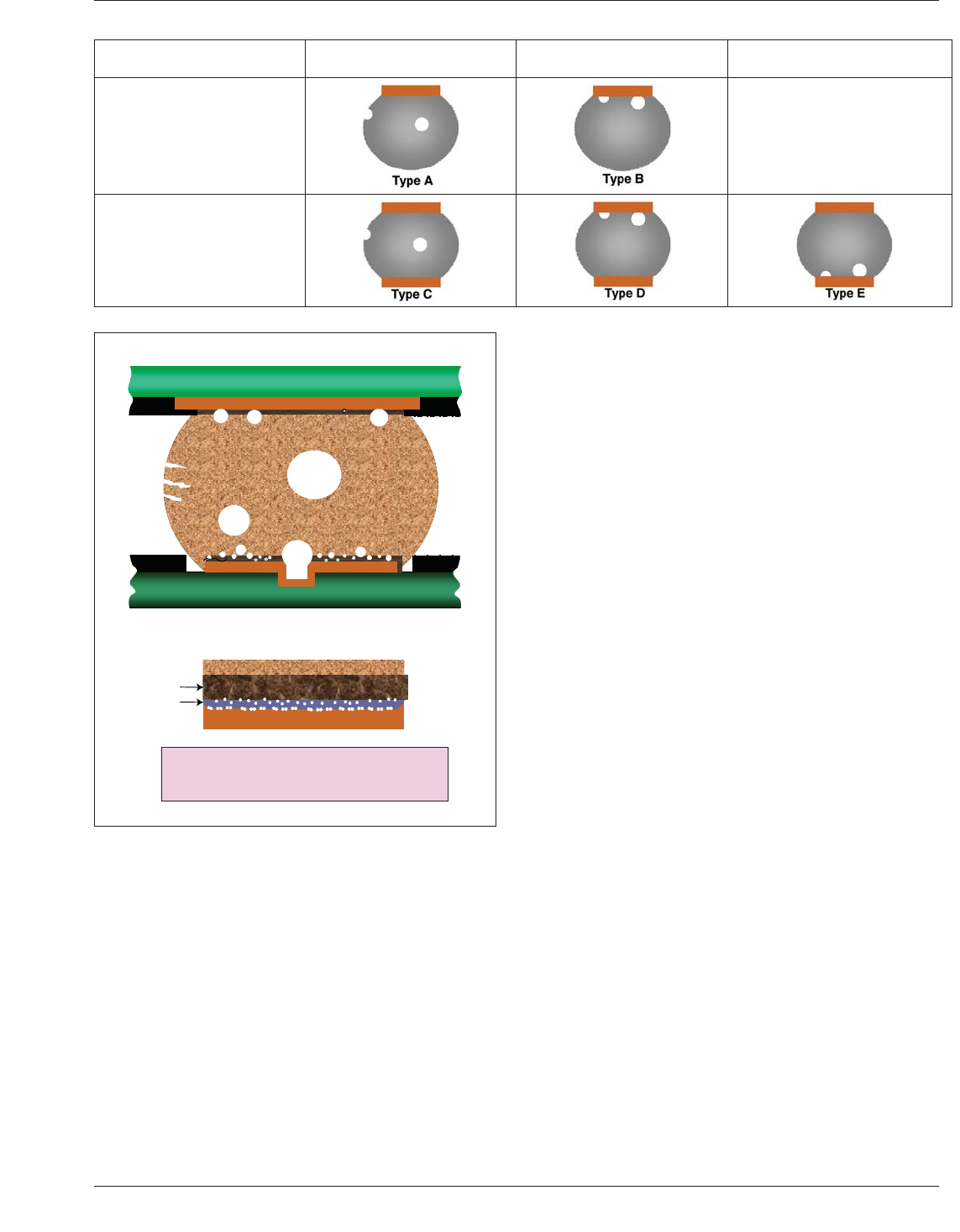
These macrovoids generally do not affect the solder joint
reliability unless they are present at interfacial regions in
the solder joints where cracks typically propagate.
7.5.3.2 Planar Microvoids Planar Microvoids are a
series of small voids, in relatively the same plane, located
at the interface between the PCB Lands and the solder.
These are caused by copper caves under ImAg surface-
finish coated lands. They do not affect initial product qual-
ity, but can affect long term solder joint reliability. They
can be eliminated by strict control of the ImAg surface fin-
ish plating solutions and etching chemicals and other criti-
cal process parameters, at all times during surface finish
plating on boards.
7.5.3.3 Shrinkage Voids Shrinkage Voids are caused by
the shrinkage during solidification, mostly for SAC and
other lead-free solders. They do not generally appear near
the solder-to-PCB land interface and do not impair the
solder joint reliability. These shrinkage voids can be mini-
mized by increasing the cooling rate during soldering and
avoiding disturbance to the joint while it’s solidifying. Fun-
damentally these shrinkage voids are surface cracks and do
not pose any reliability problems.
7.5.3.4 Microvia Voids Microvia Voids are caused by the
presence of micro-vias designed in the PCB lands. Large
Micro-via Voids, if located in solder joints in high stress
areas of a package, can impact solder joint reliability. Plat-
ing the micro-via shut, or filling it completely with solder
paste by double printing, can minimize the creation of
these voids.
7.5.3.5 IMC Microvoids IMC Microvoids occur within
the Intermetallic Compound (IMC) formed between copper
and high tin solders, including SAC and tin/lead solders.
These IMC Microvoids do not form immediately after the
soldering process, but after aging at high temperatures or
during temperature cycling of the solder joints. The true
root cause is still under investigation, but a Kirkendall
voiding mechanism may play a part. These voids can affect
solder joint reliability, particularly in instances when brittle
fracture is initiated within the IMC during drop or
mechanical shock to the solder joint. Doping the solder
with certain elements such as zinc is one way to diminish
the amount of these IMC microvoids.
7.5.3.6 Pinhole Voids Pinhole Voids are caused by pin-
holes in the copper lands of the PCB. With sufficient quan-
tity, they can affect solder joint reliability. These voids are
caused by entrapped PCB fabrication chemicals within
these pinholes that volatilize during the reflow soldering
process. The pinholes occur due to an excursion within the
copper plating process at the PCB fabricator and can
be eliminated by improved copper plating process control
systems.
Table 7-6 Void Classification
Void Analysis Voids Within the Ball
Voidsatthe
Package Interface
Voids at the Mounting
Surface Interface
Voids in BGA balls prior to
attachment to a PWB
N/A
Voids in BGA balls after
attachment to a PWB
IPC-7095c-7-43
Figure 7-43 Typical Size and Location of Various Types of
Voids in a BGA Solder Joint
1
1
1
1
1
2
2
2
4
6
6
1
1
1
1
1
2
2
2
3
5
4
6
6
BGA Solder Joint after Reflow Soldering
Cu-IMC-Solder Interface
after High Temp Aging
Cu
6
Sn
5
Cu
6
Sn
1: Macrovoids
2: Planar Microvoids
3: Shrinkage Voids
4: Micro-Via Voids
5: IMC Microvoids
6: Pinhole Voids
January 2013 IPC-7095C
103
Copyright IPC-Association Connecting Electronics Industries
Provided by IHS under license with IPC
Not for Resale
No reproduction or networking permitted without license from IHS
--`,,```,,,,````-`-`,,`,,`,`,,`---
Whenever voids are observed in solder joints, they first
need to be identified in one of the above categories, in
order to determine their impact on joint reliability and to
assess corrective actions to minimize or eliminate them.
7.6 Void Measurement
7.6.1 X-Ray Detection and Measurement Cautions
Some of the real time X-ray inspection systems still in use
for the detection of solder voids employ an X-ray imaging
device that exhibits an aberration referred to in the litera-
ture as Voltage Blooming or Phosphor Blooming. Any sys-
tem using an image intensifier or flat panel detector can, in
theory, be made to bloom. However, modern, high contrast
x-ray systems, using either image intensifiers or flat panel
detectors are more than capable of providing proper
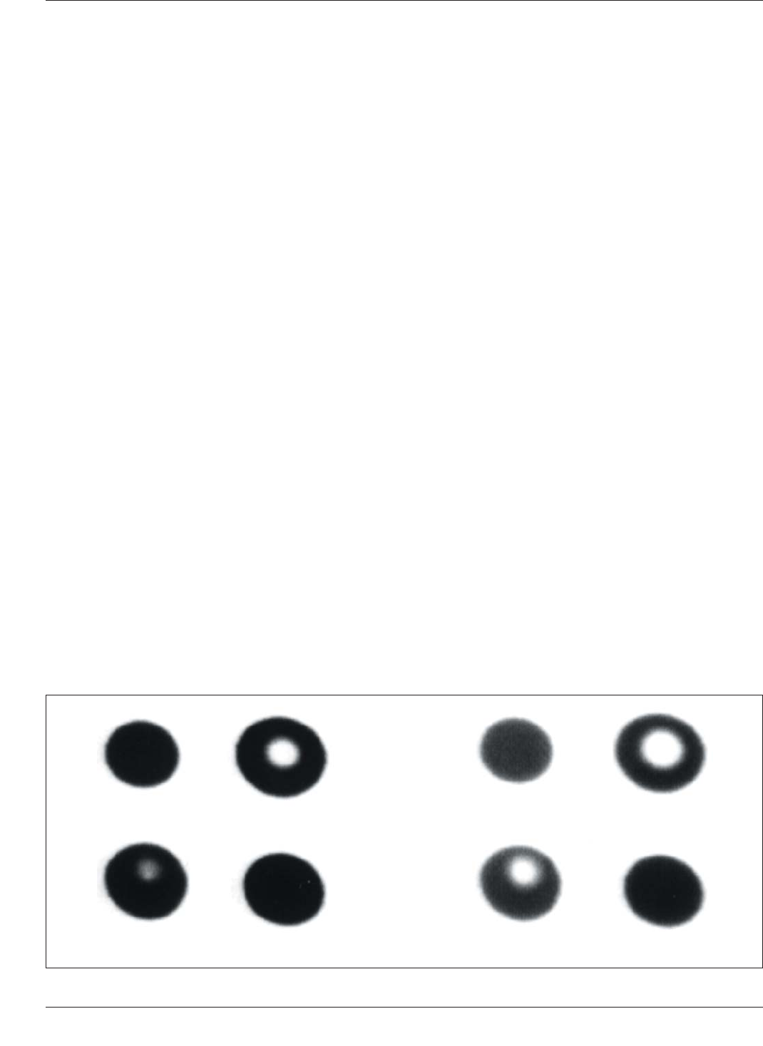
images. Figure 7-44 is an example of voltage blooming in
older systems. If it is determined that the X-ray inspection
system in use exhibits voltage blooming, the following rec-
ommendations are made to obtain a more precise measure-
ment of void size:
• X-ray film images not being subject to voltage blooming
have been found to provide a more accurate determina-
tion of void size.
• Correlation of the X-ray source voltage, to the degree of
blooming, when the actual size of a void has been deter-
mined by cross-sectioning or simulation. Note: The tonal
quality should be good enough to see a wire through the
void.
• For every voltage and current setting, the gray scale
should be reset to between 120 and 140, fora1to256
gray scale system. Normalizing gray scale will maintain
consistency between measurements.
7.6.2 Impact of Voids How many and what size of voids
should be allowable in the product before they impact the
product’s required reliability? Voids may impact reliability
by weakening the solder balls and reducing functionality
because the reduced cross-section will have lower heat
transfer and current carrying capabilities.
Large voids are more detrimental but small pre-existing
voids can merge during reflow to create large voids. The
elimination of voids, or at least a substantial reduction, is
generally preferred. The process controls to minimize void-
ing should be established during the development stage of
the process.
There are a number of studies that have shown that a small
increase in performance is observed as a result of moderate
size voids. These are typically from processes that are in
control. The increased reliability results from increased sol-
der joint height and a temporary and local retardation of
crack propagation.
X-ray inspection is required for the detection of voids in
BGA solder joints; cross-sectioning may be necessary in
order to determine the impact of the void or its location and
size.
Low cost equipment is based on transmission X-ray.
Unlike a leaded component, BGAs have solder joints that
are not only on the component’s periphery, but have inter-
nal solder joints that are not inspectable by normal visual
techniques. Higher cost equipment is based on X-ray
tomography or laminography. Both types of these systems
provide valuable techniques for void detection and location
(see 7.3.1). It is recommended that the process be qualified
for void acceptance before being released for production.
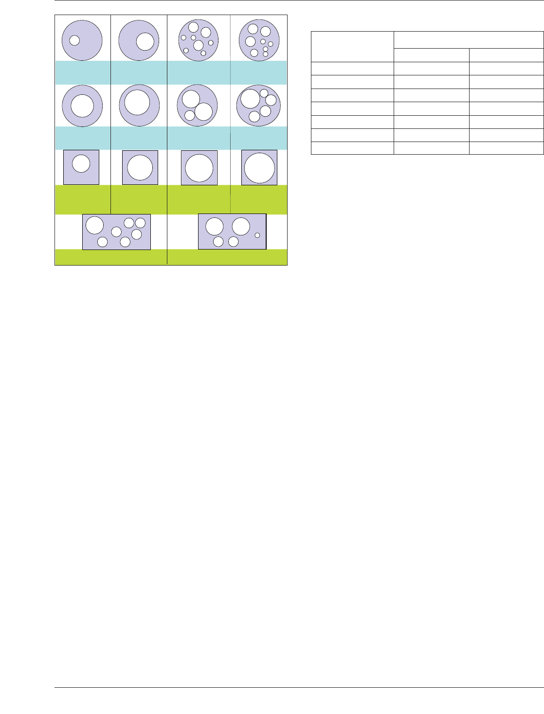
7.6.3 Void Protocol Development In many applications,
engineering teams create a void protocol which describes
the allowable voiding after the controlled experiments have
determined the characteristics of the project. Figure 7-45
shows an example of a protocol that can be established to
show the variation of void size compared to ball diameter
for various land pattern geometries.
IPC-7095c-7-44a,b
Figure 7-44 X-Ray Image of Solder Balls with Voids at 50 kV (a) and 60 kV (b)
(a) (b)
IPC-7095C January 2013
104
Copyright IPC-Association Connecting Electronics Industries
Provided by IHS under license with IPC
Not for Resale
No reproduction or networking permitted without license from IHS
--`,,```,,,,````-`-`,,`,,`,`,,`---
For in-process control, use >35% area as the threshold with
a >50% void diameter threshold. For reject-rework, use
>45% area as the criteria with a >65% void diameter
threshold.
Use of X-ray requires some caution regarding radiation
overexposure on vulnerable materials or components, as
the radiation dose from different x-ray systems can vary
widely. The implications of radiation dose to radio-
sensitive components may need to be discussed with your
component supplier and the dose rates that will be achieved
under typical x-ray inspection should be discussed with
your x-ray equipment supplier.
Although much description data is provided on identifica-
tion of voids, there is not always correlation to significant
factors related to thermal cycle life of the joint. In addition,
no data is currently available on rework vs. thermal cycle
life.
Normal area percent voids is 15 ± 10% of the projected
area.
Note: Voids at ~30% warrant process-control attention.
Voids >50% warrant rework (see Section 7.5).
Considering a 0.20 mm diameter void as an example, Table
7-7 lists the void percentages for different ball sizes. The
percentage void diameter detectable becomes larger as sol-
der joint size decreases; that is, 27% on a 0.75 mm joint
inflates to 67% on a 0.30 mm solder joint.
Defect determination is made by the product’s reliability
requirements. As an example, if the maximum allowable
void size is 31% of the solder ball diameter, the equivalent
of the void area is 9%. This can be either one void, or the
summation of many voids. Some of the newer X-ray equip-
ment use algorithms that are able to summarize the void
areas. The current algorithms for X-ray tomography do not
perform the summation of the voids.
For a single void, X-ray tomography can identify a defect
caused by a void that is greater than the pre-determined
size.
Example: If the solder ball size = 0.75 mm and the maxi-
mum allowable void size = 30% of the ball diameter, the
maximum void size at the center of the ball would be cal-
culated as follows:
30% of 0.75 mm
(0.75 mm)(0.3) = 0.225 mm maximum void diameter
When the void is not in the center of the ball and near the
land of either the board or the component, the cross-
sectional diameter of the ball will be reduced as well as the
maximum allowable size for a void.
Example: If the ball diameter at the land is approximately
equal to the land and the land size is 75% of the ball size
(25% reduction), then:
75% of 0.75 mm = 0.56 mm ball diameter at the land
30% of 0.56 mm = maximum void diameter
(0.56)(0.3) = 0.17 mm maximum void diameter
at the land
7.6.4 Sampling Plans for Void Evaluation Because of
the industry concern regarding voids, this standard attempts
to define criteria for void baseline goals and process con-
trol techniques. Everyone agrees that it makes no sense to
throw away good product, or rework product where a void
is identified without some indication as to the complexity
and the impact on reliability of that condition.
Void occurrence criteria are not based on 100% inspection,
but are accomplished through the use of sampling plans.
The sampling plan conditions are identical to those shown
in IPC-6012 and are repeated in Table 7-8. It should be
noted that the table is based on C=0. What this means is
that, as within all IPC standards, when a sample is selected,
IPC-7095c-7-45
Figure 7-45 Examples of Suggested Void Protocols
025" land 06" void
24% DIAMETER
6% AREA
025" land 013" void
52% DIAMETER
27% AREA
.020" X .030"
.010" VOID
50% DIAMETER
10% AREA
20 X 40 + 10,5,5,5,5,5,5
24% AREA
20 X 40 + 10,10,5,5,3
26% AREA
.020" X .030"
.014" VOID
70% DIAMETER
19% AREA
.020" X .030"
.016" VOID
80% DIAMETER
25% AREA
.020" X .030"
.018" VOID
90% DIAMETER
31% AREA
025" land 015" void
60% DIAMETER
36% AREA
025" land 010" void
50% DIAMETER
16% AREA
25 + 6,6,6,3,3,3,3,3
24% AREA
25 + 10,10,6
38% AREA
25 + 10,6,6,6
37% AREA
25 + 6,6,6,4,3,3,3,3
25% AREA
Table 7-7 Ball-to-Void Size Image -
Comparison for Various Ball Diameters
Solder Ball
Diameter/
X-Ray Image
Void 0.20 mm Diameter
% Void Diameter % Void Area
0.85 mm 24% 6%
0.75 mm 27% 7%
0.65 mm 31% 9%
0.55 mm 36% 13%
0.45 mm 44% 20%
0.40 mm 50% 25%
0.30 mm 67% 44%
January 2013 IPC-7095C
105
Copyright IPC-Association Connecting Electronics Industries
Provided by IHS under license with IPC
Not for Resale
No reproduction or networking permitted without license from IHS
--`,,```,,,,````-`-`,,`,,`,`,,`---