IPC-7095C-2013.pdf - 第39页
with a melting point of 302°C. The ball attachment alloy , however , may be a eutectic solder (Sn63Pb37). Although polymer encapsulation or over-molding is widely used to encase the die area, some ceramic-based BGA packa…
require peak reflow temperatures from 240-260°C, depend-
ing on the overall mass of the assembly being processed.
Depending on the specific alloy composition specified, the
liquidus point of the solder ball can vary by as much as
10°C (see Table 4-7).
Within the SnAgCu system, the addition of other alloying
elements has also been suggested; however, these additions
can affect solder under-cooling, the formation of various
intermetallics, unusual matrix properties and changes in
solder microstructure. Great care must to be taken when
introducing new alloys into BGAs and new alloyed BGAs
into the assembly process. Outside the SnAgCu system,
various alloy systems containing Bi, In, Sb or Zn have also
been developed. The underlying metallurgy of each system
differs, which drives the physical properties and mechani-
cal behavior; thus, assembly process parameters and solder
joint reliability.
4.4.2 Ball Attach Process The package substrate is typi-
cally fabricated in a strip format containing multiple pack-
ages (see Figure 4-7). Ball contact placement is performed
after they have gone through wire bonding and plastic
molding or encapsulation process steps. Both automated
and semi-automated ball placement is being utilized for
volume BGA assembly. Alloy spheres of the desired size
(as shown in Table 4-1) are attached either by gang place-
ment machines, individually placed using automated sys-
tems, or dispensed in mass with a stencil-like fixture. For
companies doing development or for low-volume place-
ment, simple template fixtures can be provided for precise
ball positioning. The overall ball attachment process, how-
ever, is the same. To begin, liquid or ‘‘tacky’’ paste flux is
dispensed or printed onto the contact pattern. The flux
holds the balls in place during reflow soldering. Reflow
soldering of the ball to the substrate is often performed in
a nitrogen gas environment. The nitrogen gas environment
helps provide consistent ball quality and keeps the surface
from oxidizing during reflow. However, nitrogen gas may
not be necessary for reflow attachment of the package to
the PCB. The eutectic solder balls provide a ‘‘controlled
collapse’’ that, during reflow soldering, promotes self-
alignment (compensating for some misplacement during
assembly).
There are some issues to consider when using plastic BGA
packages. The first is moisture sensitivity. Moisture sensi-
tive components around other components being removed
and replaced during rework must be dried in advance
and/or protected from the heat of the rework activity. If the
plastic cased BGA is to be re-used then special care will be
required to re-ball the BGA after the package is detached
from the board assembly. Moisture sensitivity is not the
case with the high melting point noncollapsing balls used
on ceramic based BGA; also the balls do not melt during
rework.
The plastic BGA package is also susceptible to warpage
when exposed to temperatures required for solder attach-
ment. The edges of the package tend to lift up or curve
down during reflow soldering and can severely disturb or
interrupt the electrical interface between package and board
assembly. The larger packages are even more susceptible to
warpage than the smaller packages. The package warpage
is caused by CTE mismatch between the substrate struc-
ture, the mold compound and the silicon die inside. This
problem may become more acute when the die is large, or
when the BGA has a heat spreader.
4.4.3 Ceramic Ball Grid Array The internal connections
in the ceramic-based package can be either wire-bond or
flip-chip. Figure 4-8 shows flip-chip bonding inside the
package. The package can be furnished with the die
mounted on the top surface of the substrate (cavity up) or
with the die mounted to the substrate’s lower surface (cav-
ity down). The solder balls generally used for ceramic
packages typical of that illustrated in Figure 4-9 are a high
temperature alloy composition (90% lead and 10% tin)
Table 4-7 Pb-Free Alloy Variations
Composition Alloy
Liquidus
Temperature
Reflow
Temperature
Sn96.5/Ag3.5 Tin/Silver 221°C 240-250°C
Sn99.3/Cu0.7 Tin/Copper 227°C 245-255°C
Sn93.6/Ag4.7/
Cu1.7
Tin/Silver/
Copper*
216°C 237-247°C
Sn95/Ag4.0/
Cu1
Tin/Silver/
Copper*
218°C 238-248°C
Sn96.5/Ag3.0/
Cu0.5
Tin/Silver/
Copper*
218°C 238-248°C
Sn95.5/Ag4.0/
Cu0.5
Tin/Silver/
Copper
218°C 238-248°C
Sn95.5/Ag3.8/
Cu0.7
Tin/Silver/
Copper
218°C 238-248°C
Sn96.3/Ag3.2/
Cu0.5
Tin/Silver/
Copper
218°C 238-248°C
Sn95.75/Ag3.5/
Cu0.75
Tin/Silver/
Copper*
218°C 238-248°C
* May be covered by patents
IPC-7095c-4-7
Figure 4-7 Plastic Ball Grid Array (BGA) Package
Die
Package
Substrate
Package
Substrate
Wire Bond
IPC-7095C January 2013
24
Copyright IPC-Association Connecting Electronics Industries
Provided by IHS under license with IPC
Not for Resale
No reproduction or networking permitted without license from IHS
--`,,```,,,,````-`-`,,`,,`,`,,`---
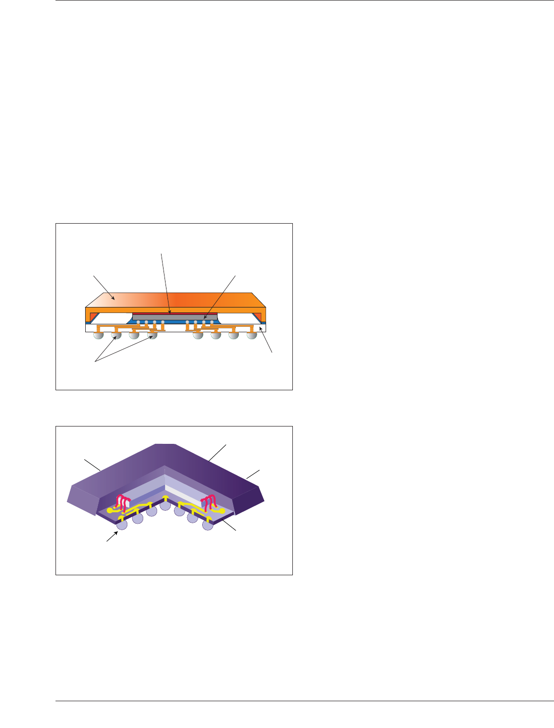
with a melting point of 302°C. The ball attachment alloy,
however, may be a eutectic solder (Sn63Pb37).
Although polymer encapsulation or over-molding is widely
used to encase the die area, some ceramic-based BGA
packaged devices are hermetic (do not absorb moisture).
Since solder balls often adapted for these products have a
high melting point, they do not collapse during rework.
The disadvantage of the ceramic-based BGA is that its high
thermal mass will be slightly different than the plastic
packaged ICs and can make solder reflow profile develop-
ment more difficult. Because of the CTE mismatch between
the ceramic-based package and the circuit board, the solder
joints may need to be physically reinforced. Following the
soldering and cleaning process, it is a common practice to
apply an epoxy based underfill between ceramic substrate
interposer and organic PCB materials.
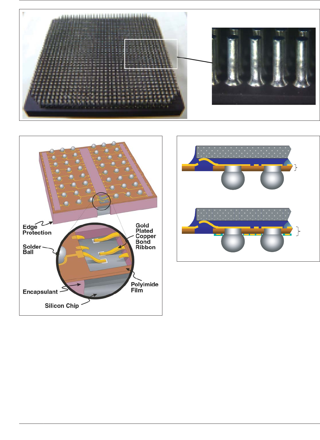
4.4.4 Ceramic Column Grid Arrays Solder column con-
tacts typical of that illustrated in Figure 4-10 are used for
larger ceramic-based packages (32 mm to 45 mm). The
package resembles the earlier pin-grid-array but with closer
contact pitch and more fragile leads (columns). The column
contact diameter is approximately 0.5 mm with its length
varying from 1.25 mm to 2.0 mm. The columns are
attached to the package either by eutectic (Sn63Pb37) sol-
der or they are cast in place using 90% lead and 10% tin.
The longer columns typically increase solder joint reliabil-
ity by absorbing a great deal of the thermal expansion mis-
match between the ceramic package and the board.
Longer columns, on the other-hand, may reduce electrical
performance and will increase the overall package height
profile. The columns are not as rugged as ball contacts and
are susceptible to handling damage.
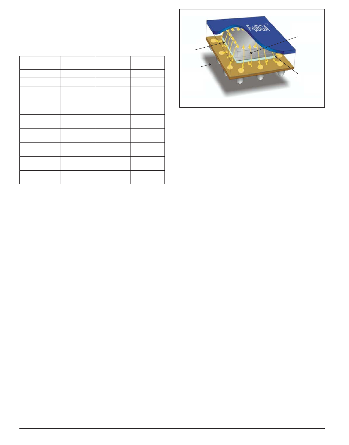
4.4.5 Tape Ball Grid Arrays A tape (polyimide film)
based ball grid array, illustrated in Figure 4-11, can furnish
a lower overall profile package. The low dielectric polyim-
ide film can be furnished with one or two metal layers for
high density in-package circuit routing.
For polyimide interposer-based BGAs, typical of that illus-
trated, the CTE mismatch is not an issue since the die
attach adhesive and substrate flexibility will take up strains
within the package structure. Tape-based BGAs can adapt
flip-chip, wire-bond or lead-bond to achieve die-to-
substrate interconnection. The single metal layer tape sub-
strate is typically used for low cost and low lead count
package applications and the two metal layer tape for
higher lead count or performance driven applications.
An additional layer of copper, for example, can provide an
efficient ground return, significantly lowering inductance
and reducing the effects of switching noise. The ground
plane effect impacts noise level reduction as well, but the
number of current sinks within the ground plane will also
influence inductance levels. The two metal layer substrate
compared in Figure 4-12 not only furnishes better electri-
cal performance, it also provides a significant improvement
in in-package circuit routability.
Circuit routing of the single metal material is limited to the
narrow gap of dielectric between ball contact attachment
sites. As the contact pitch reduces down to 0.50 mm, the
space between contact features is reduced to 75 µm, pro-
viding the possibility of routing only a single circuit trace.
This factor limits the use of the single metal layer to a nar-
row band of low I/O package applications.
4.4.6 Multiple Die Packaging Portable and wireless
electronics represent the most aggressive growth area for
high-density package technology. In both circuit board fab-
rication and IC packaging, the technology for compressing
even the most sophisticated electronic functions into a
smaller and lighter finished product continues to evolve.
Portable or handheld electronics are a natural target. Digi-
tal cameras and camcorders, for example, must consider
ease of use, lighter weight and performance. Cellular
phones, pagers, personal communicators, palm top comput-
ers, industrial and automotive electronics, personal GPS,
medical and diagnostic products, are all viable candidates
for more efficient device miniaturization.
IPC-7095c-4-8
Figure 4-8 Cross-Section of a Thermally Enhanced
Ceramic Ball Grid Array (CBGA) Package
Metal Alloy
Heat Spreader
Thermal Interface
Material (TIM)
Flip Chip
Mounted
Semiconductor
Chip
Ceramic Alumina
Substrate Base
Solder Balls
IPC-7095c-4-9
Figure 4-9 Ceramic Ball Grid Array (CBGA) Package with
Molded Polymer Encapsulation
Encapsulant
Solder Ball
(Lead Free)
Ceramic
Substrate
(Double Side)
Bonding
Wire
Chip
January 2013 IPC-7095C
25
Copyright IPC-Association Connecting Electronics Industries
Provided by IHS under license with IPC
Not for Resale
No reproduction or networking permitted without license from IHS
--`,,```,,,,````-`-`,,`,,`,`,,`---
Memory devices such as Flash, SRAM and SDRAM are
the first commodity type products in the market to adapt
FBGA and CSP in high volume. However, digital signal
processors, controllers, CPUs and any number of applica-
tion specific IC devices are also prime candidates for mul-
tiple die packaging. Many of the multiple die packages
adapt a simple wire-bond process for die-to-substrate inter-
face. The die and wire bond area is then encapsulated or
over-molded to furnish the single package outline. Wire-
bond solutions are capable of furnishing a two or more die
stack, but package height increases significantly with each
added die layer.
Two or more ICs encased in a single package outline is
more efficient in both size-to-function ratio and may
enhance performance. Multiple die packaging potentially
increases component density and improves component-to-
component circuit routing efficiency on the printed board.
Some of the multiple die package methodologies attach one
die on top of the other on a single substrate as illustrated
in Figure 4-13.
Die stacking different size die in a pyramid fashion is com-
mon but, when the die are the same size, a spacer must be
added between each active die to clear the wire-bond loop.
4.4.7 System-in-Package (SiP) To provide space for the
additional functions companies are combining a number of
related functions into a single package outline. Although
Figure 4-10 Ceramic-Based Column Grid Array (CCGA) Package
IPC-7095c-4-11
Figure 4-11 Polyimide Film-Based Lead-Bond µBGA Pack-
age Substrate Furnishes Close Coupling Between Die Pad
and Ball Contact
IPC-7095c-4-12
Figure 4-12 Comparing In-Package Circuit Routing Capa-
bility of the Single Metal Layer Tape Substrate to Two Metal
Layer Tape Substrate
Single
Metal
Tape
Two
Metal
Tape
IPC-7095C January 2013
26
Copyright IPC-Association Connecting Electronics Industries
Provided by IHS under license with IPC
Not for Resale
No reproduction or networking permitted without license from IHS
--`,,```,,,,````-`-`,,`,,`,`,,`---