IPC-7095C-2013.pdf - 第162页
10 GLOSSARY AND ACRONYMS AABUS As Agreed Upon Between User and Supplier ASIC Applications Specific IC ASM Array Surface Mount ASMP Application Specific Module Packaging AXI Automatic X-Ray Inspection BGA Ball Grid Array BO…
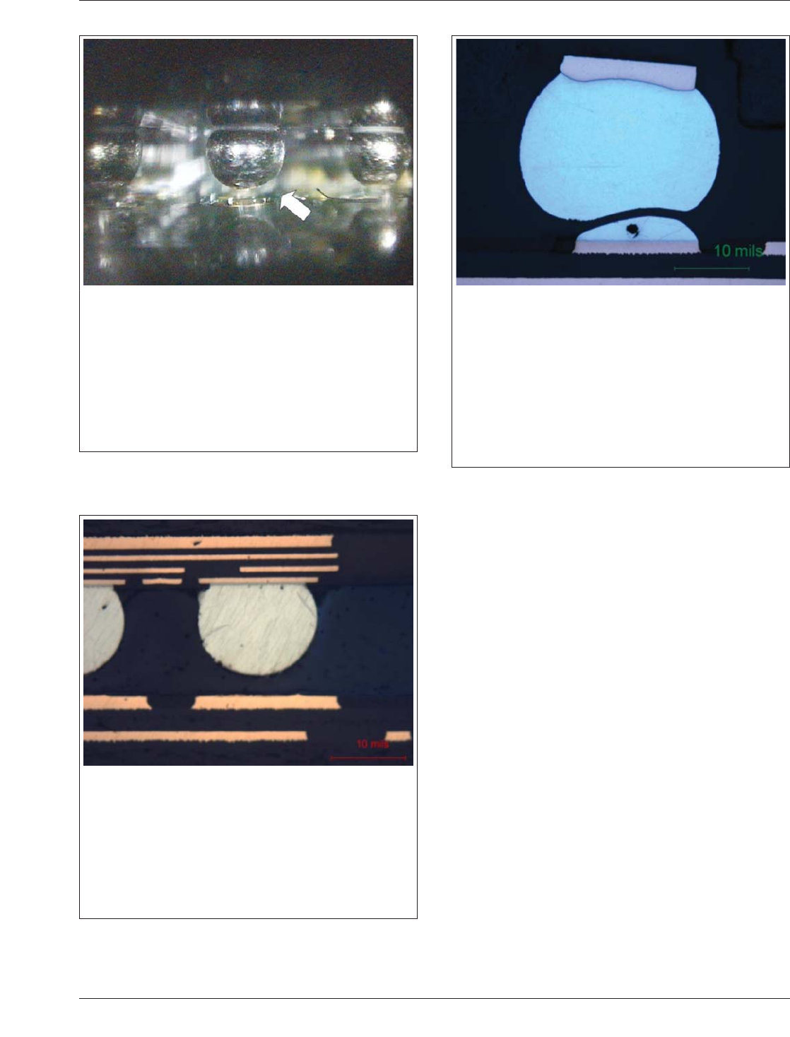
9.4.15 Missing Solder
9.4.16 Nonwet Open (NWO) Solder Joint
9.4.17 Head-on-Pillow (HoP) Solder Joint
Possible Cause
The condition is a result of package missing solder paste
deposit on the PCB land(s). The presence of the solder paste
deposit is necessary to form the BGA solder joint. This solder
paste deposit would melt during reflow soldering and coalesce
with the molten BGA solder to form the solder joint.
Potential Solution
Check stencil aperture for clogging with solder paste. Also.
ensure that the stencil is designed correctly with each aperture
opening for each SMT land on the PCB.
Possible Cause
Clogged stencil aperture, interaction between BGA warpage
and solder paste type.
Potential Solution
– Monitor paste volume using automated inspection system.
– Selection of right solder paste material/formulation to over-
come defect.
– Overprinting solder paste in risk area (BGA package corners).
– Minimizing board warpage (e.g., use of pallets).
Possible Cause
Interaction between BGA and PCB warpage, Reduced Tal at
Reflow.
Potential Solution
– Overprint solder paste in risk area (BGA package corners).
– Minimize Delta Temp within component and Increased Peak
Temperature and Time Above Liquidus (TAL) in reflow.
– Reflow in nitrogen (N
2
) ambient.
– Selection of right solder paste material/formulations to over-
come defect.
– Minimizing board warpage (e.g., use of a pallet).
January 2013 IPC-7095C
147
Copyright IPC-Association Connecting Electronics Industries
Provided by IHS under license with IPC
Not for Resale
No reproduction or networking permitted without license from IHS
--`,,```,,,,````-`-`,,`,,`,`,,`---

10 GLOSSARY AND ACRONYMS
AABUS As Agreed Upon Between User and
Supplier
ASIC Applications Specific IC
ASM Array Surface Mount
ASMP Application Specific Module Packaging
AXI Automatic X-Ray Inspection
BGA Ball Grid Array
BOC Board-On-Chip
BT Bismaleimide-Triazine
CAGE Commercial and Government Entity
CBGA Ceramic Ball Grid Array
CCGA Ceramic Column Grid Array
CGA Column Grid Array
COB Chip-On-Board
CPU Central Processing Unit
CSP Chip Scale Packages
CTE Coefficient of Thermal Expansion
CTF Critical To Function
DBDPE Decabromodiphenyl Ether
DDR-
SDRAM
Double-Data-Rate Synchronous Dynamic
Random Access Memory
Df Dissipation Factor
DfM Design for Manufacturability
DfR Design for Reliability
DIG Direct Immersion Gold
Dk Dielectric Constant
DMA Dynamic Mechanical Analysis
DSBGA Die-Size Ball Grid Array
DSC Differential Scanning Calorimetry
DSP Die Size Package
dT Temperature Differential
ECM Electrochemical Migration Test
ENEPIG Electroless Nickel/Electroless Palladium/
Immersion Gold
ENIG Electroless Nickel Immersion Gold
ESD Electrostatic Discharge/Electrostatic Device
ESS Environmental Stress Screening
EU European Union
FAT Flux Activation Time
FBGA Fine Pitch Ball Grid Array
FC Flip Chip
FPT Fine Pitch Technology
FRBGA Fine-Pitch, Rectangular Ball Grid Array
FT Functional Test
GAC Grid Array Component
HASL Hot Air Solder Level
HAST Highly Accelerated Stress Testing
HCI Hydrochloric
HDB High Density Printed Boards
HF Hydrofluoric
HoP Head-on-Pillow
I/O Input/Output
ICT In-Circuit Test
ILC Independent Loading Mechanism
IMC Intermetallic Compound
IR Infrared
LCP Liquid Crystal Polymer
LFBGA Low-Profile Fine-Pitch Ball Grid Array
LMC Least Material Condition
LTD Liquidus Time Delay
MCM Multichip Module
MCM-L Multichip Module-Laminate
MCP Multichip Package
MD Metal Defined
MDA Manufacturing Defect Analyzer
MDS Multi Device Subassembly
MLC Multilayer Ceramic
MMB Moisture Membrane Bag
MMC Maximum Material Condition
NAND Not ‘‘And’’
NSMD Nonsolder Mask Defined
OEM Original Equipment Manufacturer
OSP Organic Solderability Preservative
PBB Polybrominated Biphenyl
PBBO Polybrominated Biphenyl Oxide
PBDE Polybrominated Diphenyl Ether
PBGA Plastic Ball Grid Array
PCA Printed Circuit Assembly
PCB Printed Circuit Board
PCM Phase Change Materials
PCMCIA Personal Computer Memory Card
International Association
PGA Pin Grid Array
PLCC Plastic Leaded Chip Carrier
PSA Pressure Sensitive Adhesives
PTH Plated Through-Hole
QFP Quad Flat Pack
RDS Rectangular Die Size
RF Radio Frequency
IPC-7095C January 2013
148
Copyright IPC-Association Connecting Electronics Industries
Provided by IHS under license with IPC
Not for Resale
No reproduction or networking permitted without license from IHS
--`,,```,,,,````-`-`,,`,,`,`,,`---

RFID Radio Frequency Identification
RMS Root Mean, Square
RoHS Restriction of Hazardous Substances
RSS Ramp-Soak-Spike
RTS Ramp-to-Spike
SAC Sn/Ag/Cu
SDRAM Synchronous Dynamic Random Access
Memory
SGA Solder Grid Array
SIR Surface Insulation Resistance
SMD Solder Mask Defined
SMOBC Solder Mask Over Bare Copper
SMT Surface Mounting Technology
SO-DIMM Small Outline Dual In-Line Memory
Module
SOIC Small Outline Integrated Circuit
SPC Statistical Process Control
SRAM Static Random Access Memory
SSO Simultaneously Switching Output
STII Soldering Temperature Impact Index
TAB Tape-Automated Bonding
TAL Time Above Liquidus
TBBPA Tetrabromobisphenol A
TBGA Tape Ball Grid Array
Td Decomposition Temperature
TFBGA Thin Profile Fine Pitch Ball Grid Array
T
g
Transition Temperature
TIM Thermal Interface Materials
TMA Thermal Mechanical Analysis
UFPT Ultra Fine Pitch Technology
UtRAM Uni-transistor Random Access Memory
UUT Unit Under Test
UV Ultraviolet
VFBGA Very Thin-Profile Fine-Pitch Ball Grid Array
WEEE Waste in Electrical and Electronic
Equipment
ZIF Zero Insertion Force
January 2013 IPC-7095C
149
Copyright IPC-Association Connecting Electronics Industries
Provided by IHS under license with IPC
Not for Resale
No reproduction or networking permitted without license from IHS
--`,,```,,,,````-`-`,,`,,`,`,,`---