IPC-7095C-2013.pdf - 第63页
One side T ype a T wo sides T ype b T ented V ia (T ype I Via) A via with a dry film mask material applied bridging over the via wherein no additional materials are in the hole. It may be applied to one side. (T ype I-a) …

damage the via wall resulting in open vias. However,
applying the via caps after the surface finish has been
applied can degrade some surface finishes (e.g., OSP,
ImAg, ImSn) due to the thermal exposure that is necessary
to cure the via cap material. Both of these issues must be
taken into account when making a decision to flood or cap
vias. Most PCB suppliers flood or cap vias before the sur-
face finish is applied.
There are presently eight different methods of via plugging/
capping identified in IPC standardization. These are shown
in Figure 5-12. It is important to realize that the choice of
tented, plugged and filled vias for via protection can have
direct impacts on the subsequent assembly processes.
Table 5-4 provides the pros and cons of tenting, plugging
and filling vias. The choice among the options presented
will depend on the capabilities of both the fabricators and
the assemblers. To avoid complication during assembly, it
is imperative that all involved in the manufacturing process
understand the trade-offs among the options.
5.5 Thermal Spreader Structure Incorporation (e.g.,
Metal Core Boards)
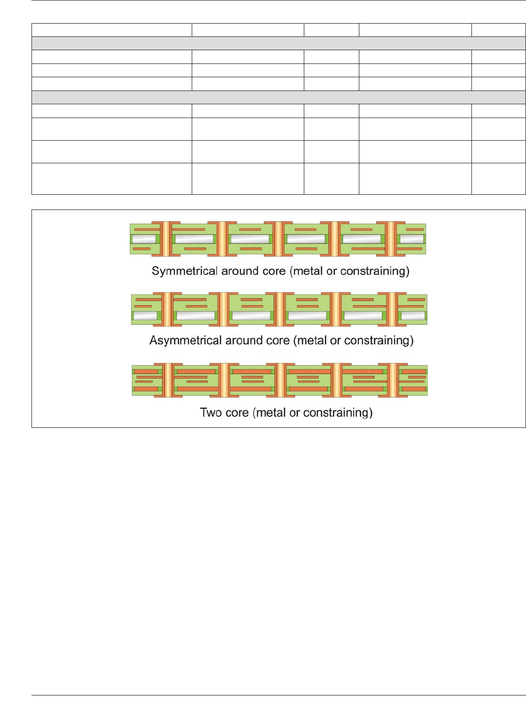
When structural, thermal, or electri-
cal requirements dictate, a conductive constraining core or
metal core can be inserted into the layer structure. It is rec-
ommended that the board circuitry layer configuration is
made symmetrical about the the core as the center. It is
possible to create structures that are asymmetrical (i.e.,
having a different number of layers to either side of the
core); however, plated-through holes going through the
entire stack may be less reliable due to the differences in
expansion on either side of the metal or constraining core
(see Figure 5-13).
One reason for asymmetrical design is the separation of
electrical functions from mechanical or thermal functions,
but this advantage might be offset by board distortion or
warping during soldering operations (or during thermal
cycling in the intended operating environment) due to dif-
ferences in the thermal expansion of materials.
Some compensation can be achieved by having additional
copper planes added to the back of the interconnection
product. The extra copper plane may increase the expan-
sion coefficient slightly and make soldering more difficult
due to the need to put more energy into the board to assure
proper solder joint formation; however, a positive effect is
that it enhances thermal conductivity.
5.5.1 Lamination Sequences As previously noted, more
desirable constructions are those where circuit layers are
symmetrical about the core chosen to serve at the center of
the board. By so doing, individual multilayer circuits can
be produced separately, each with their own laminating
sequence. For example, a four layer board might be manu-
factured having vias through the entire four layers and this
can be duplicated for use on either side of the core.
To achieve mechanical constraint within a chosen and use-
ful range, the total thickness of the core in the multilayer
should be approximately 25% of the board’s total thick-
ness. Constraining core board is more often used because
the core layers may be imaged, etched, and connected to
the plated-through hole. The thicker center core must be
machined. Better thermal cycle survival has been shown in
some studies for structures having two constraining cores
in the board rather than one.
Another configuration is to have a special constraining core
board made by bonding a multilayer board to each side of
a thick metal core after each of the boards has been com-
pleted. The composite board is then sequentially drilled,
plated, and etched to form plated-through hole connections
between the two boards. Coupons should be provided to
test the integrity of the composite structure.
5.5.2 Heat Transfer Pathway Metal core boards add sig-
nificantly to the thermal mass of the assembly. This may
force the preheating soldering process to be operated at
abnormally high limits. These designs should be thor-
oughly evaluated under production conditions prior to
release. Laminate ruptures and discoloration and grainier
textured solder are typical effects that have been observed.
The heat transfer path between components and the planes
are usually accomplished through either direct contact with
the plane or through thermal vias positioned under the
component and connected to the thermal core or plane in
its position.
Table 5-3 Via Filling/Encroachment to Surface Finish Process Evaluation
Surface Finish Tenting Flooding Capping Plugging Encroaching
HASL Okay Okay Okay Okay Okay
OSP Okay Not Recommended Okay Okay Okay
ENIG Okay Okay Okay Okay Okay
ImAg Okay Not Recommended Okay Okay Okay
ImSn Okay Not Recommended Okay Okay Okay
IPC-7095C January 2013
48
Copyright IPC-Association Connecting Electronics Industries
Provided by IHS under license with IPC
Not for Resale
No reproduction or networking permitted without license from IHS
--`,,```,,,,````-`-`,,`,,`,`,,`---
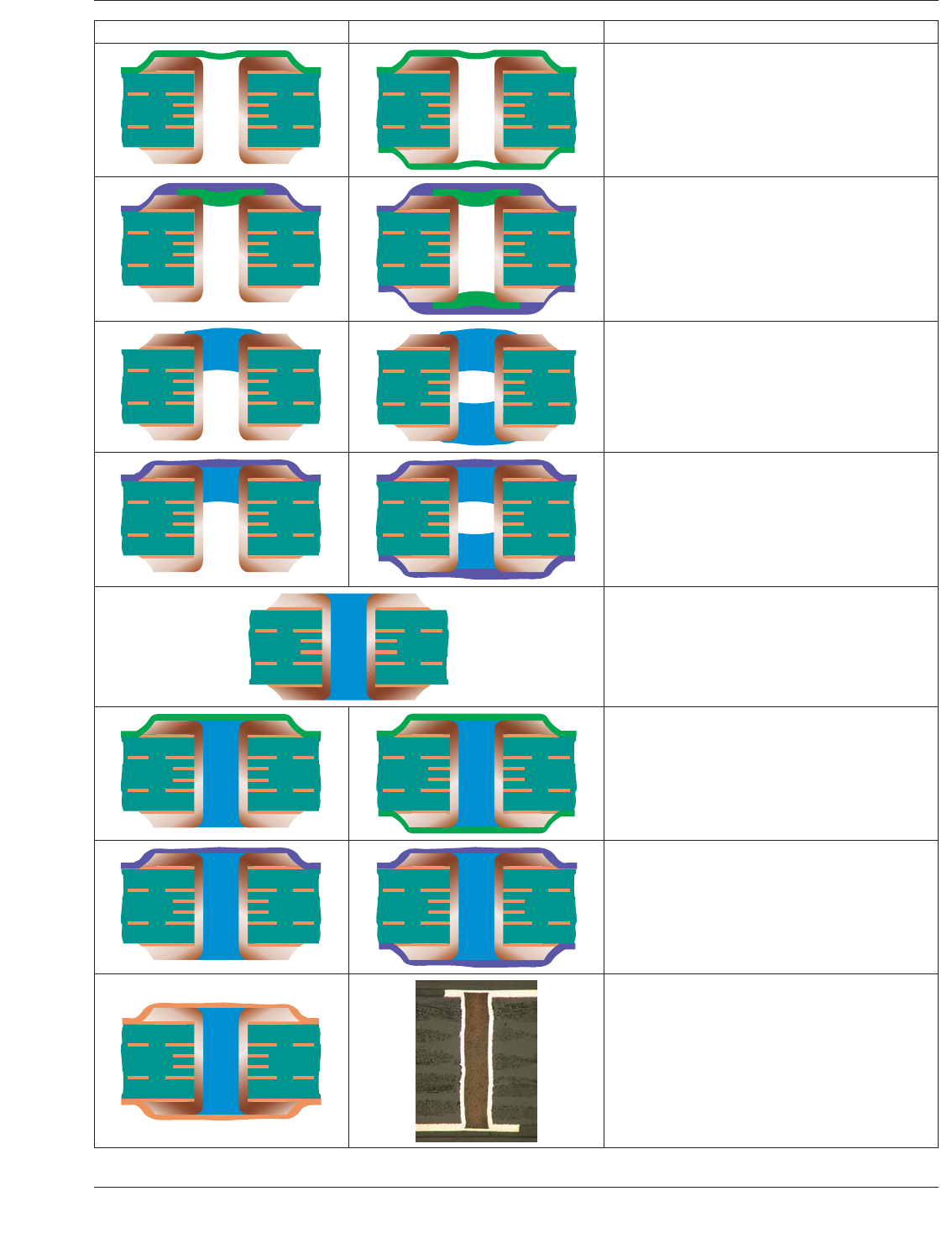
One side Type a Two sides Type b
Tented Via (Type I Via)
A via with a dry film mask material applied
bridging over the via wherein no additional
materials are in the hole. It may be applied
to one side.
(Type I-a) or both sides (Type I-b) of the via
structure (IPC-4761, Figure 5-1).
Tented and Covered Via (Type II Via)
A Type I via with a secondary covering of mask
material applied over the tented via. The material
may be applied to one side (Type II-a) or both
sides (Type II-b) of the via structure (IPC-4761,
Figure 5-2).
Plugged Via (Type III Via)
A via with material applied allowing partial
penetration into the via. The plug material
may be applied from either one side (Type III-a)
or both sides (Type III-b) of the via structure
(IPC-4761, Figure 5-3).
Plugged and Covered Via (Type IV Via)
A Type III via with a secondary covering of
material applied over the via. The plug and
secondary covering material may be applied
from either one side (Type IV-a) or both sides
(Type IV-b) of the via structure (IPC-4761,
Figure 5-4).
Filled Via (Type V Via)
A via with material applied into the via targeting
a full penetration and encapsulation of the hole
(IPC-4761, Figure 5-5).
Filled and Covered Via (Type VI Via)
A Type V via with a secondary covering of
material (liquid or dry film soldermask) applied
over the via. The covering material may be
applied from either one side (Type VI-a) or
both sides (Type VI-b) of the via structure
(IPC-4761, Figure 5-6).
Filled and Capped Via (Type VII Via)
A Type V via with a secondary metallized
coating covering the via. The metallization
is on both sides (IPC-4761, Figure 5-7).
Partially Filled Via
The illustrations show a via filled with
nonconductive epoxy and then plated
over with copper. This is commonly
used for via in pad applications
(IPC-4761, Figure 5-8).
Figure 5-12 Via Plug Methods
January 2013 IPC-7095C
49
Copyright IPC-Association Connecting Electronics Industries
Provided by IHS under license with IPC
Not for Resale
No reproduction or networking permitted without license from IHS
--`,,```,,,,````-`-`,,`,,`,`,,`---
6 PRINTED CIRCUIT ASSEMBLY DESIGN CONSIDER-
ATION
6.1 Component Placement and Clearances
It is recom-
mended that sufficient clearance (3 mm to 5 mm) be pro-
vided around BGAs to facilitate rework. The high-end
clearances are recommended, especially for CBGA when
using a step stencil to deposit solder paste and using hot air
for rework. However, if using diode laser systems for
rework the spacing can be reduced to 0.5 mm to 1.0 mm
since laser rework does not impact adjacent components.
6.1.1 Pick and Place Requirements An advantage of
BGA packages over other advanced, high-pin count pack-
ages (fine pitch, TAB, PGA, etc.) is the ability to be placed
using existing surface mount placement equipment. BGAs
are more forgiving in the pick-and-place process because
they self-align.
6.1.2 Repair/Rework Requirements Repair/rework of
BGA components is a major driver for component spacing
requirements. A typical BGA rework method requires five
steps:
1) heating the solder joints to reflow temperatures for
package removal;
2) removal and clean-up of solder on the BGA land pat-
tern;
3) application of new solder paste or flux;
4) placement of the new BGA package;
5) heating the solder joints to reflow temperatures for
assembly of the BGA component to the circuit board.
A keepout area may be needed for each of these steps.
Rework equipment manufacturers can provide specific
details regarding necessary keepout areas. General rules are
outlined below.
Table 5-4 Via Fill Options
Top Bottom Top & Bottom No Plug
Pros
Increase rework robustness Yes Yes Yes No
Reduce secondary reflow risk at wave Yes Yes Yes No
Prevent solder drain Yes Yes Yes No
Cons
Secondary Fab process Yes Yes Yes No
Component side height profile restriction
less than 50 µm
above solder mask
No
less than 50 µm
above solder mask
No
Flux contaminant concern
Yes – (if exposed to
wave solder directly)
No No No
Plug integrity concern
Yes (tented, plugged)
No (filled)
Yes (tented,
plugged)
No (filled)
Yes (tented, plugged)
No (filled)
No
IPC-7095c-5-13
Figure 5-13 Metal Core Board Construction Examples
IPC-7095C January 2013
50
Copyright IPC-Association Connecting Electronics Industries
Provided by IHS under license with IPC
Not for Resale
No reproduction or networking permitted without license from IHS
--`,,```,,,,````-`-`,,`,,`,`,,`---